Structures and methods for coupling energy from an electromagnetic wave

a technology of electromagnetic waves and coupling energy, applied in the field of coupling energy from electromagnetic waves, can solve the problems of difficult manufacturing, large size of structures needed to create electromagnetic radiation at a desired frequency, and limited success,

Inactive Publication Date: 2009-07-07
ADVANCED PLASMONICS
View PDF307 Cites 15 Cited by
  • Summary
  • Abstract
  • Description
  • Claims
  • Application Information

AI Technical Summary

Problems solved by technology

As frequencies increase, however, the kinds of structures needed to create the electromagnetic radiation at a desired frequency become generally smaller and harder to manufacture.
By around 1960, people were trying to reduce the size of resonant structures to get even higher frequencies, but had limited success because the Q of the devices went down due to the resistivity of the walls of the resonant structures.
Higher levels of radiation are generally thought to be prohibitive because resistance in the cavity walls will dominate with smaller sizes and will not allow oscillation.
Also, using current techniques, aluminum and other metals cannot be machined down to sufficiently small sizes to form the cavities desired.
There is no practical magnetic field strong enough to keep the electron spinning in that small of a diameter at those speeds.
Small recognizes this issue but does not disclose a solution to it.
Smith-Purcell devices are inefficient.
Their production of light is weak compared to their input power, and they cannot be optimized.
Current Smith-Purcell devices are not suitable for true visible light applications due at least in part to their inefficiency and inability to effectively produce sufficient photon density to be detectible without specialized equipment.
We realized that the Smith-Purcell devices yielded poor light production efficiency.
Currently, LEDs and Solid State Lasers (SSLs) cannot be integrated onto silicon (although much effort has been spent trying).
Further, even when LEDs and SSLs are mounted on a wafer, they produce only electromagnetic radiation at a single color.

Method used


Image

  • Structures and methods for coupling energy from an electromagnetic wave
  • Structures and methods for coupling energy from an electromagnetic wave
  • Structures and methods for coupling energy from an electromagnetic wave

Examples


Embodiment Construction

Brief Description of the Figures

[0046]The invention is better understood by reading the following detailed description with reference to the accompanying drawings in which:

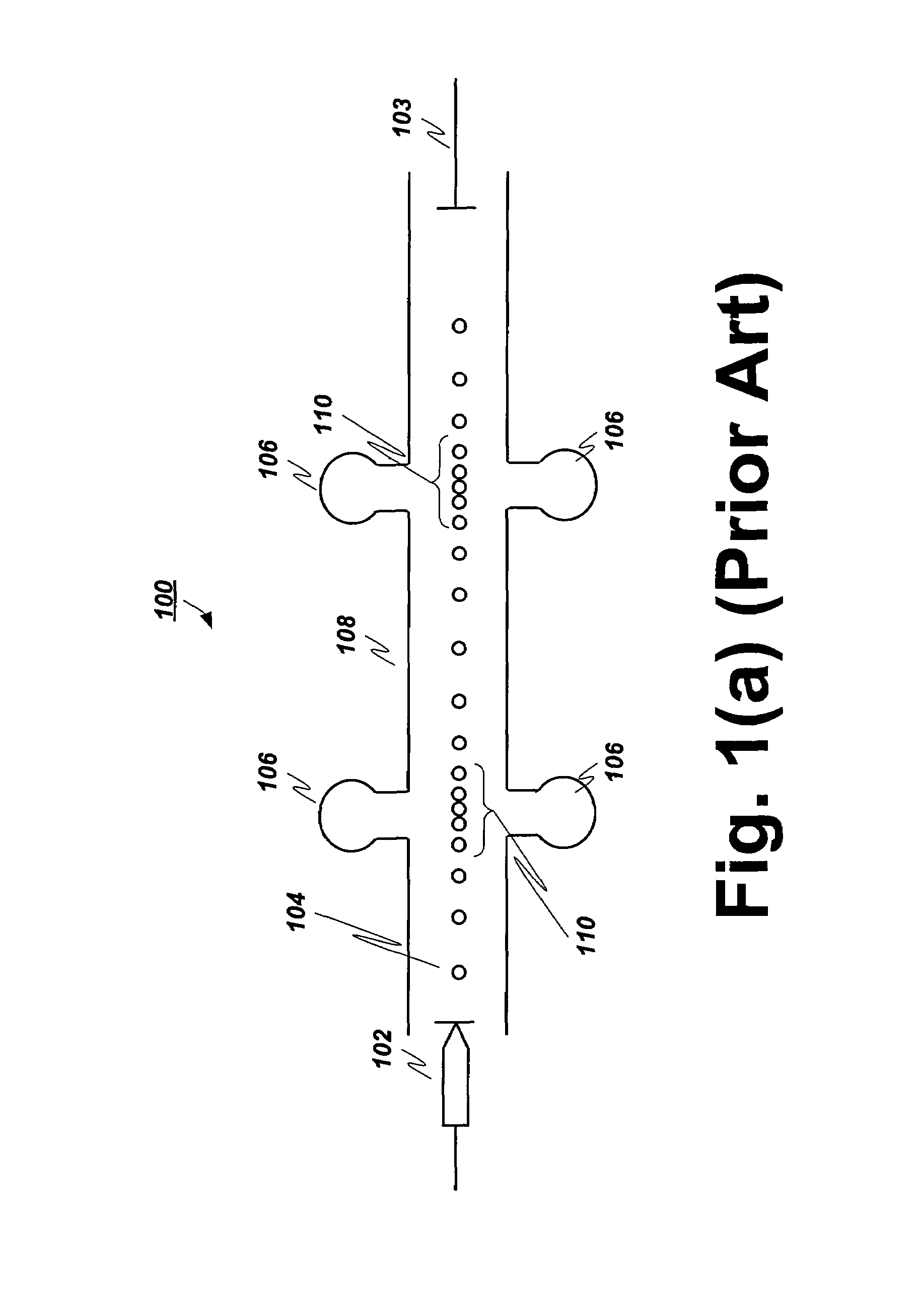
[0047]FIG. 1(a) shows a prior art example klystron.

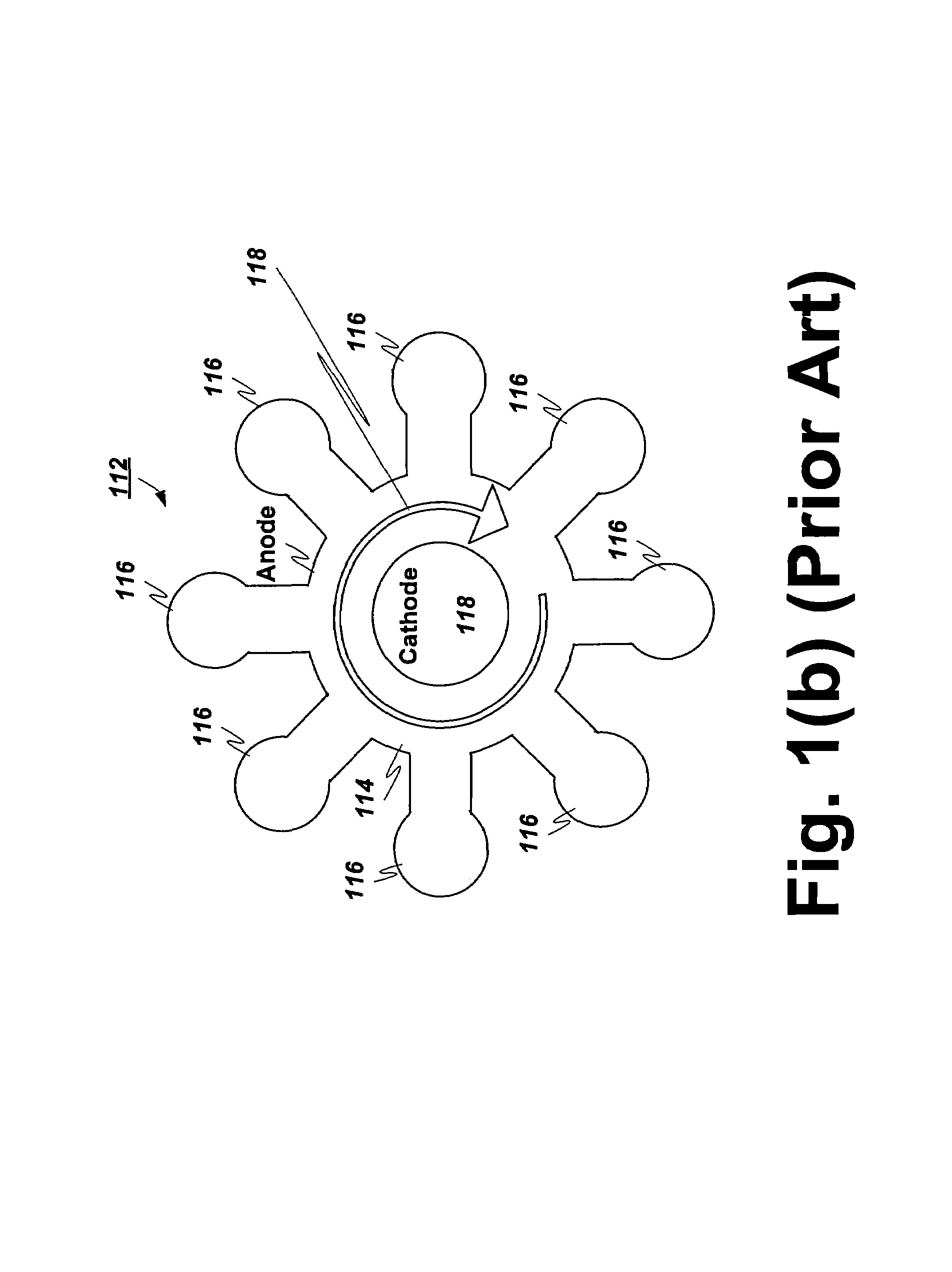
[0048]FIG. 1(b) shows a prior art example magnetron.

[0049]FIG. 1(c) shows a prior art example reflex klystron.

[0050]FIG. 1(d) depicts aspects of the Smith-Purcell theory.

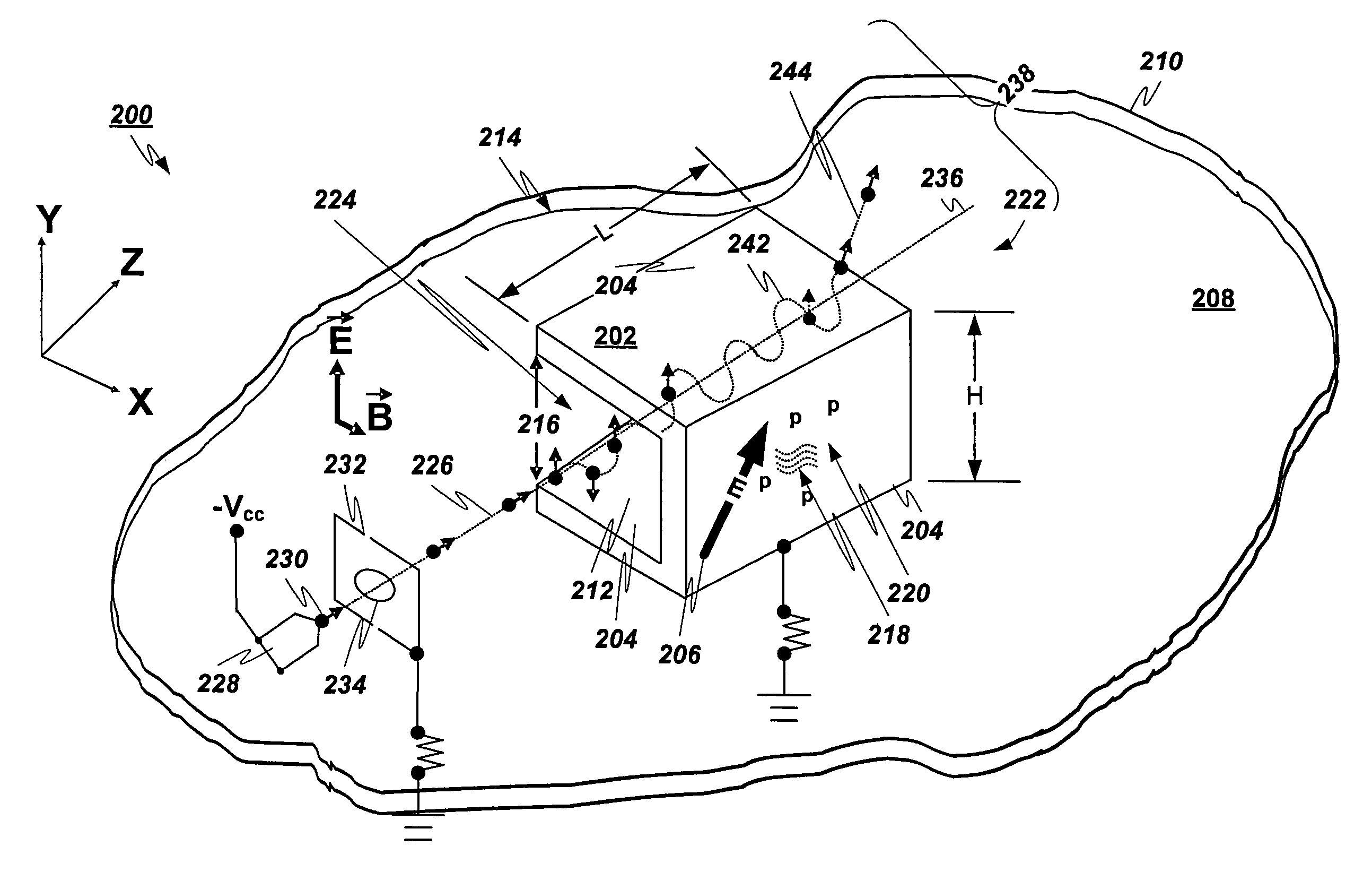
[0051]FIG. 2(a) is a highly-enlarged perspective view of an energy coupling device showing an ultra-small micro-resonant structure in accordance with embodiments of the present invention;

[0052]FIG. 2(b) is a side view of the ultra-small micro-resonant structure of FIG. 2(a);

[0053]FIG. 3 is a highly-enlarged side view of the energy coupling device of FIG. 2(a);

[0054]FIG. 4 is a highly-enlarged perspective view of an energy coupling device illustrating the ultra-small micro- resonant structure according to alternate embodiments of the present invention;

[0055]FIG. 5 is a highly-enlarged perspective v...


PUM

PropertyMeasurementUnit
diameteraaaaaaaaaa
diameteraaaaaaaaaa
diameteraaaaaaaaaa

Abstract

A device couples energy from an electromagnetic wave to charged particles in a beam. The device includes a micro-resonant structure and a cathode for providing electrons along a path. The micro-resonant structure, on receiving the electromagnetic wave, generates a varying field in a space including a portion of the path. Electrons are deflected or angularly modulated to a second path.

Description

RELATED APPLICATIONS[0001]This application is continuation of U.S. patent application Ser. No. 11 / 243,476, titled “Structures and Methods for Coupling Energy from an Electromagnetic Wave, ” file Oct. 5, 2005, the entire contents of which are incorporated herein by reference. This application is related to and claims priority from U.S. patent application Ser. No. 11 / 238,991, titled “Ultra-Small Resonating Charged Particle Beam Modulator,” and filed Sep. 30, 2005, the entire contents of which are incorporated herein by reference. This application is related to U.S. patent application Ser. No. 10 / 917,511, filed on Aug. 13, 2004, entitled “Patterning Thin Metal Film by Dry Reactive Ion Etching,” and U.S. application No. 11 / 203,407, entitled “Method Of Patterning Ultra-Small Structures,” filed on Aug. 15, 2005, and U.S. application Ser. No. 11 / 243,477, titled “Electron Beam Induced Resonance,” and filed on Oct. 5, 2005, all of which are commonly owned with the present application at the ...

Claims


Application Information

Patent Timeline
Patent Type & Authority Patents(United States)
IPC IPC(8): G01J1/00
CPCH01J25/34
Inventor GORRELL, JONATHANDAVIDSON, MARKGASPAROV, LEV V.MAINES, MICHAEL E.HART, PAUL
Owner ADVANCED PLASMONICS
Why Eureka
Try Eureka