DRAM controller for graphics processing operable to enable/disable burst transfer

a dram controller and graphics processing technology, applied in static indicating devices, memory adressing/allocation/relocation, instruments, etc., can solve the problems of significant overhead, increase the refresh time of the sdram access bandwidth, and insufficient technique to solve, so as to reduce the number of cycles required for dram access.

Active Publication Date: 2009-07-14
SOCIONEXT INC
View PDF20 Cites 197 Cited by
  • Summary
  • Abstract
  • Description
  • Claims
  • Application Information

AI Technical Summary

Benefits of technology

[0056]According to this invention, in processing which extends across the neighboring drawing blocks, for example, in a write operation of a rectangle extending across the boundary between the neighboring drawing blocks, since the different DRAMs are assigned to those neighboring drawing blocks, issuance of, e.g., active commands alternately to the DRAMs reduces the number of command-issue waiting cycles resulting from the issue interval restriction. Furthermore, the burst transfer control unit outputs the individual signals for stopping burst transfers to the DRAMs. Therefore, when the processing has passed across the boundary between the drawing blocks, the write to or the read from the DRAM assigned to the previous drawing block can be reliably stopped, requiring no cycle for stopping the burst transfer. This reduces overhead caused when the processing passes across the boundary between the drawing blocks. As a result, the DRAM access is executed with a smaller number of cycles as compared with the conventional case.
[0064]In the inventive DRAM controller, in processing in which the plurality of frame-buffer areas are used, issuance of, e.g., active commands alternately to the DRAMs reduces the number of command-issue waiting cycles resulting from the issue interval restriction, because the different DRAMs are assigned to those frame-buffer areas. Furthermore, the burst transfer control unit outputs the individual signals for stopping burst transfers to the DRAMs. Therefore, when the frame-buffer area is switched from one to another, the write to or the read from the DRAM assigned to the previous frame-buffer area can be reliably stopped, requiring no cycle for stopping the burst transfer. This reduces overhead occurring when the plurality of frame-buffer areas are used. As a result, the DRAM access is executed with a smaller number of cycles as compared with the conventional case.
[0067]As described above, according to the present invention, in processing that extends across drawing blocks, or in processing in which a plurality of frame-buffer areas are used, the number of cycles required for DRAM access can be reduced as compared with the conventional case.

Problems solved by technology

On the other hand, a disadvantage of SDRAM is that when access is made in no order of address, a precharge command and an active command have to be input to the SDRAM every time such access is made.
It is thus apparent that significant overhead occurs in, e.g., display processing or processing in which a large amount of line segment data is written, if addresses and pixel data are simply associated with each other on a one-to-one basis.
However, there still remains a problem with the conventional technique in that significant overhead may occur when DRAM is accessed in some processing, which means that the conventional technique has been insufficient to solve the above problem.
In this case, as in the case of FIG. 26, one reason for causing overhead is that a write command has to be issued in succession in each cycle, and a precharge command and an active command cannot be issued together with the write command.
In addition, along with the trend toward increasingly greater amounts of process data, SDRAM capacity also increases correspondingly, resulting in an increase in refresh time in the SDRAM access bandwidth.

Method used


Image

  • DRAM controller for graphics processing operable to enable/disable burst transfer
  • DRAM controller for graphics processing operable to enable/disable burst transfer
  • DRAM controller for graphics processing operable to enable/disable burst transfer

Examples


first embodiment

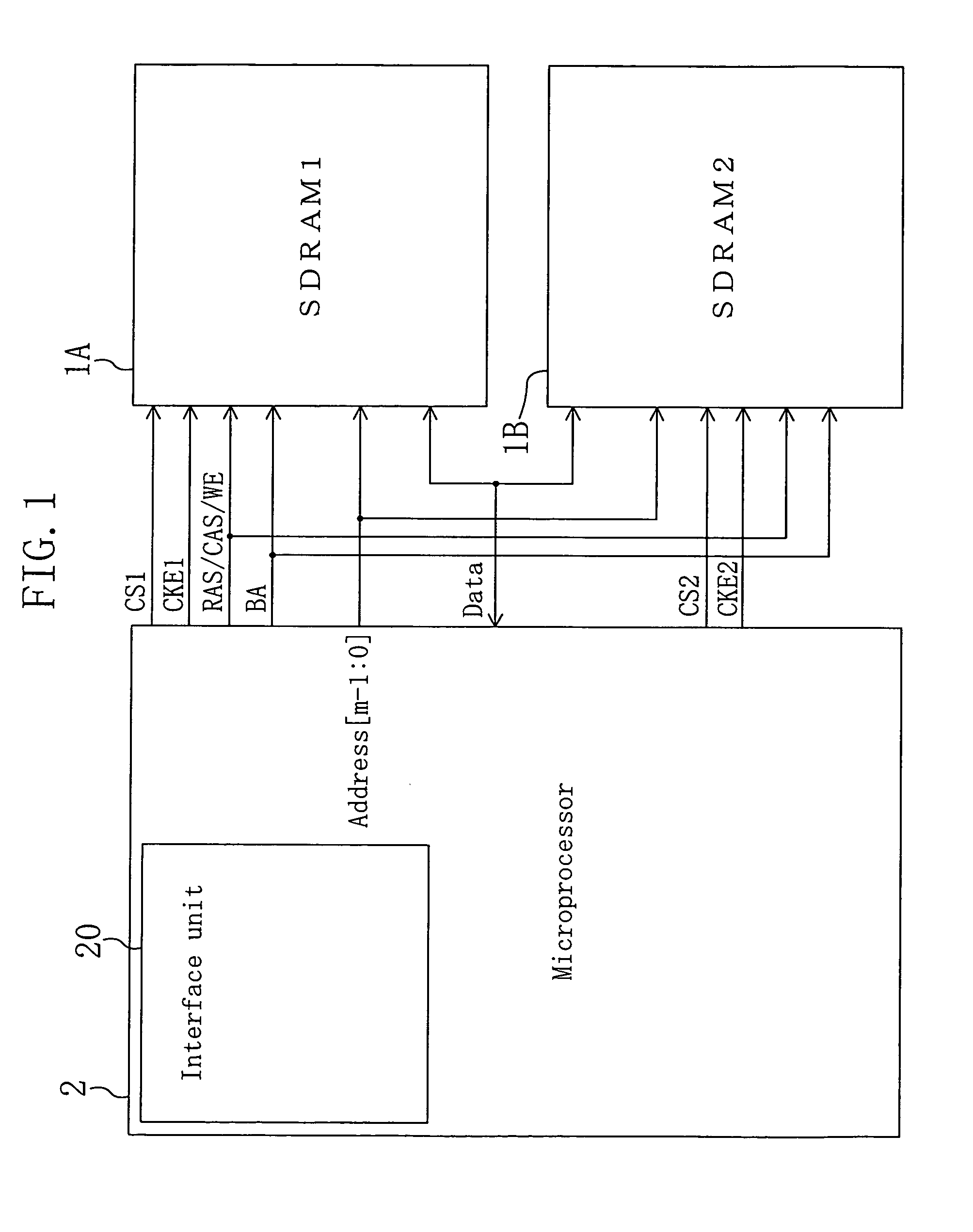
[0097]FIG. 1 illustrates a schematic configuration of a DRAM controller in accordance with a first embodiment of the present invention. In FIG. 1, a first SDRAM 1A (SDRAM1) and a second SDRAM 1B (SDRAM2) are connected to a microprocessor 2. An interface unit 20 provided in the microprocessor 2 assigns a frame-buffer area to the first and second SDRAMs 1A and 1B and accesses the first and second SDRAMs 1A and 1B in accordance with graphics processing such as drawing processing and display processing.

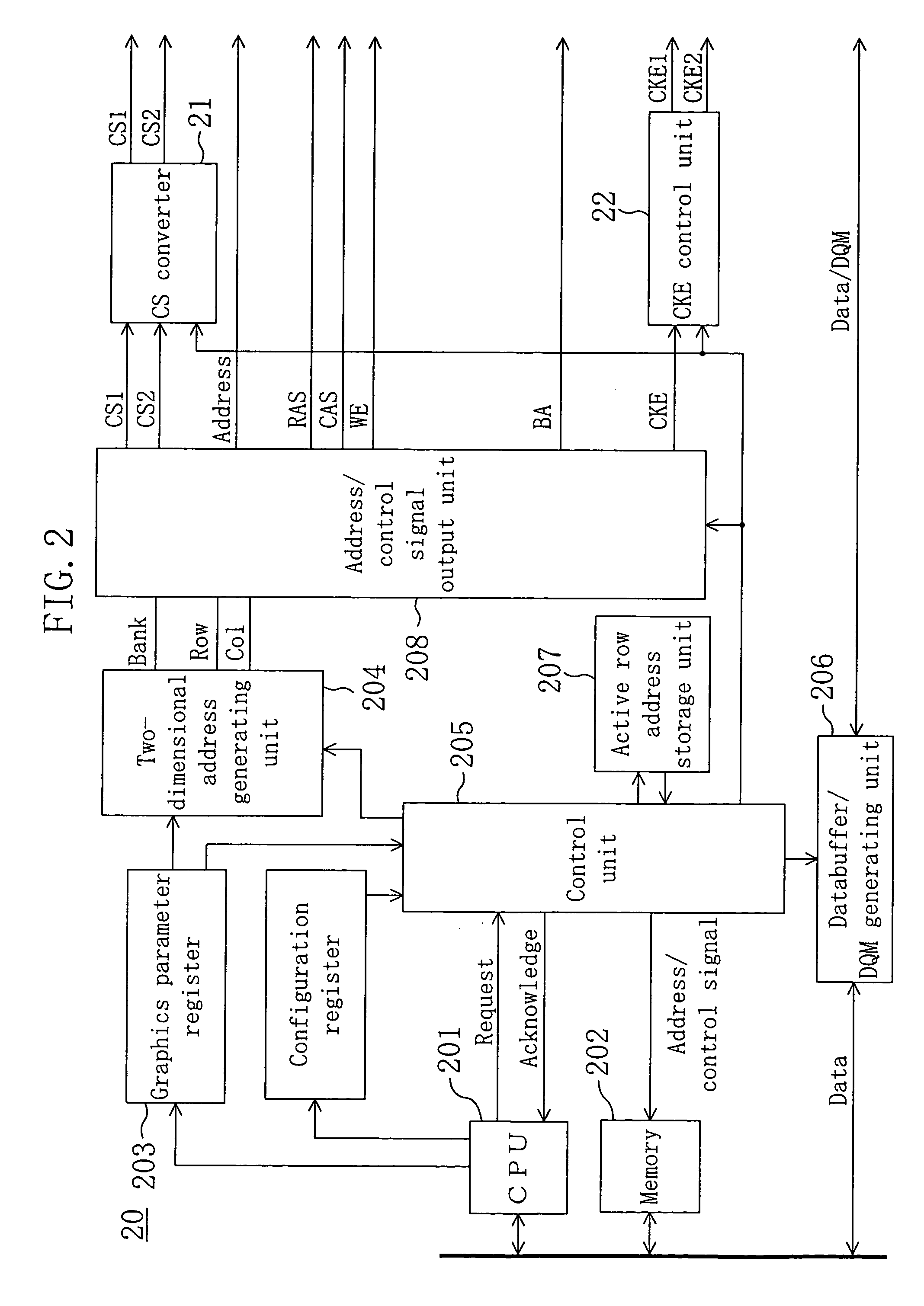
[0098]FIG. 2 is a block diagram illustrating the configuration of the interface unit 20 of FIG. 1. In FIG. 2, components common to those in the conventional configuration shown in FIG. 21 are identified by the same reference numerals and the detailed description thereof will be omitted herein. The reference numeral 21 denotes a CS (chip select signal) converter and 22 denotes a CKE (clock enable signal) control unit. The CKE control unit 22, serving as a burst transfer control unit, outpu...

second embodiment

[0114]FIG. 10 illustrates a schematic configuration of a DRAM controller in accordance with a second embodiment of the present invention. FIG. 11 is a block diagram illustrating the configuration of an interface unit 20B of FIG. 10. In FIGS. 10 and 11, components common to those shown in FIGS. 1 and 2 are identified by the same reference numerals and the detailed description thereof will be omitted herein. In FIG. 11, a BA (bank select signal) control unit 81 outputs individual first and second bank select signals BA1 and BA2 to first and second SDRAMs 1A and 1B, respectively. An AS (address select signal) control unit 82 receives the 0th bit of an address output from an address / control-signal output unit 208 and outputs individual first and second address select signals AS1 and AS2 to the first and second SDRAMs 1A and 1B, respectively. The remaining bits of the address other than the 0th bit are supplied to both first and second SDRAMs 1A and 1B. The address / control-signal output ...

third embodiment

[0129]FIG. 14 illustrates a schematic configuration of a DRAM controller in accordance with a third embodiment of the present invention. FIG. 15 is a block diagram illustrating the configuration of an interface unit 20C of FIG. 14. In FIGS. 14 and 15, components common to those shown in FIGS. 1 and 2 or FIGS. 10 and 11 are identified by the same reference numerals and the detailed description thereof will be omitted herein.

[0130]In FIG. 15, a control signal control unit 111, serving as a command control unit, receives a RAS signal, a CAS signal and a WE signal output from an address / control signal control unit 208, and in order to issue individual commands to first and second SDRAMs 1A and 1B, the control signal control unit 111 outputs control signals RAS1, CAS1 and WE1 and control signals RAS2, CAS2 and WE2 to the first and second SDRAMs 1A and 1B, respectively.

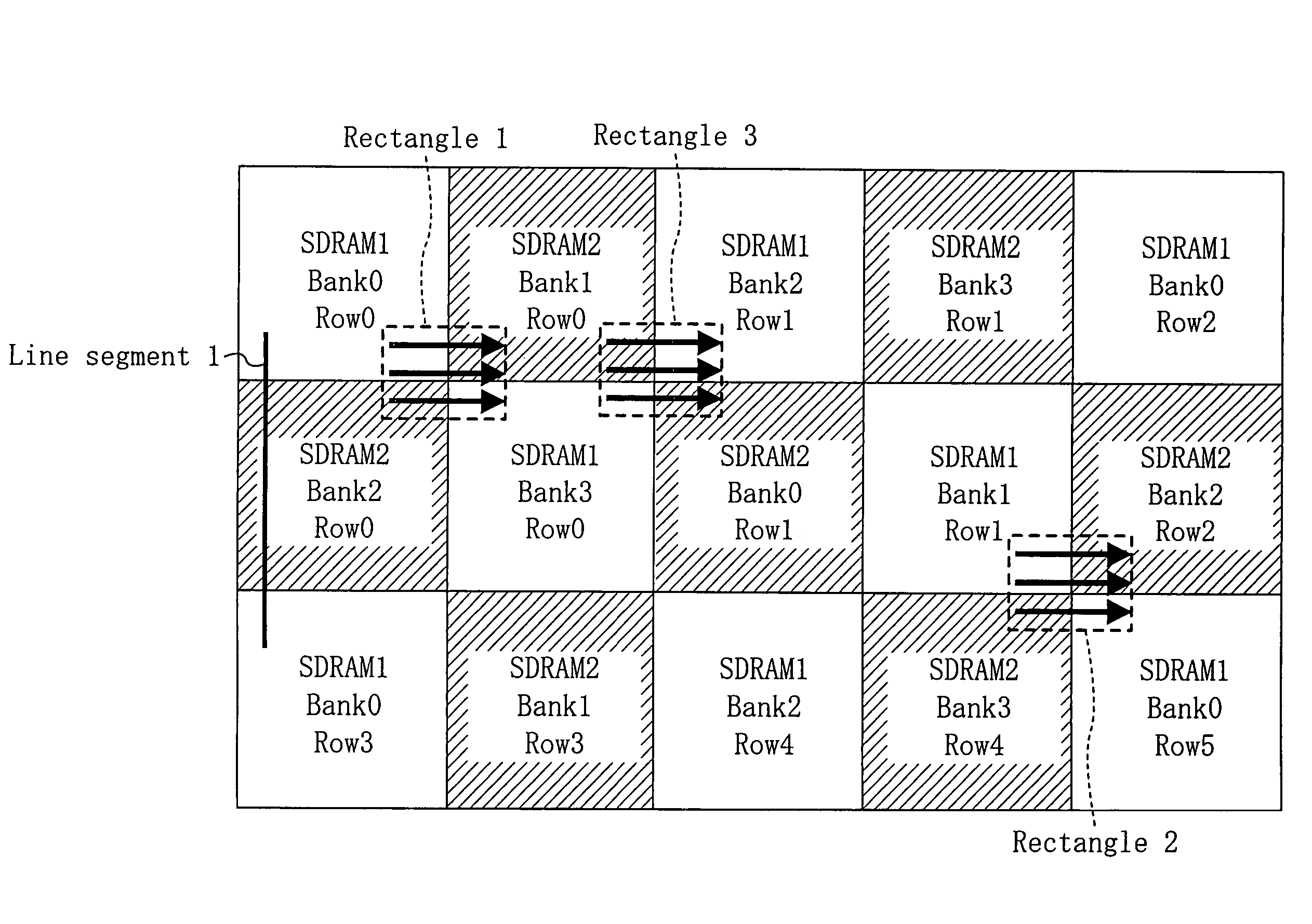
[0131]It is assumed that frame-buffer-area address mapping in this embodiment is performed as shown in FIG. 3 as in the f...


PUM


Abstract

An interface unit 20 assigns different SDRAMs 1 and 2 to adjacent drawing blocks in a frame-buffer area. In processing that extends across the adjacent drawing blocks, active commands, for example, are issued alternately to the SDRAMs 1 and 2 to reduce waiting cycles resulting from the issue interval restriction. Furthermore, since individual clock enable signals CKE1 and CKE2 are output to the SDRAMs 1 and 2 so that burst transfers of the SDRAMs 1 and 2 can be stopped individually, no cycle is necessary to stop the burst transfers.

Description

CROSS-REFERENCE TO RELATED APPLICATION[0001]This application is related to Japanese Patent Application No. 2004-2275 filed on Jan. 7, 2004, whose priority is claimed under 35 USC §119, the disclosure of which is incorporated herein by reference in its entirety.BACKGROUND OF THE INVENTION[0002]The present invention relates to technology for controlling access to DRAMs capable of burst transfers, for the purpose of, e.g., graphics processing.[0003]In most of the current graphics processors, a dedicated video memory is not used, and instead a frame-buffer area is provided, together with other process data, in an SDRAM (synchronous DRAM) for cost reduction. In those graphics processors, to write graphic data into the frame-buffer area, the pixel positions and pixel data of the graphic data are calculated and the pixel data is written into the frame-buffer area in the SDRAM in accordance with the pixel positions. On the other hand, to display drawing data stored in the frame-buffer area ...

Claims


Application Information

Patent Timeline
Patent Type & Authority Patents(United States)
IPC IPC(8): G06F12/00G06F12/02G06F12/06G06F13/00G06F13/28G06F13/372G09G5/36G09G5/39G06F13/16G06T1/00G09G5/393G11C7/10G11C8/00
CPCG09G5/363G09G5/393G11C7/1042G09G2360/128
Inventor HENMI, MASANORIKURATA, KAZUSHI
Owner SOCIONEXT INC
Why Eureka
Try Eureka