Semiconductor device package and method for manufacturing same

a technology of semiconductor devices and semiconductor devices, applied in semiconductor devices, semiconductor/solid-state device details, electrical apparatus, etc., can solve the problems of affecting package performance, requiring a relatively long length of bond wire, and longer length of bond wir

Active Publication Date: 2009-07-21
UNISEM M BERHAD
View PDF22 Cites 25 Cited by
  • Summary
  • Abstract
  • Description
  • Claims
  • Application Information

AI Technical Summary

Problems solved by technology

One drawback to this configuration is that it requires a relatively long length of bond wire 18 to connect I / O pads on the die 14 to the leads 10.
The use of longer lengths of bond wire 18 adversely affects package performance by increasing the electrical resistance between the die 14 and the lead 10.
Also, the bond wire 18 is relatively expensive and fragile and, therefore, the use of greater amounts of bond wire 18 is undesirable.
This problem is exacerbated by the industry trend toward the use of smaller and smaller die sizes for the same size package, which increases the length of bond wire 18 for a given package size.
However, the configuration of FIG. 2 is itself problematic in that it is difficult to maintain the coplanarity of the bond sites on the interposer 20 when bonding the die to the leads.
The use of this configuration for flip-chip bonding methods also presents the problem of maintaining coplanarity of the bond sites on the interposers 20 when bonding the die 14 to the leads 10.
The use of ultrasonic bonding in such modern encapsulation techniques is problematic for a number of reasons.
For example, the leads 10 formed on modern lead frames are very thin and are therefore easily broken by the aluminum wedge bonding process.

Method used


Image

  • Semiconductor device package and method for manufacturing same
  • Semiconductor device package and method for manufacturing same
  • Semiconductor device package and method for manufacturing same

Examples


Embodiment Construction

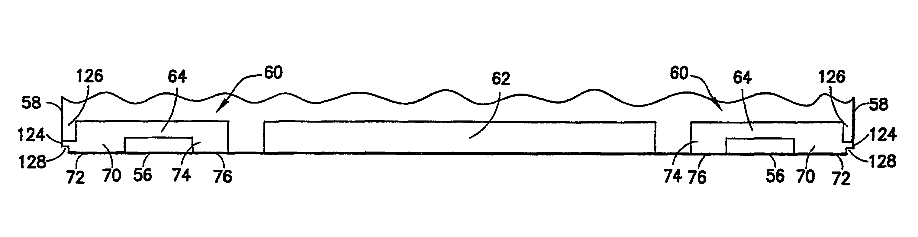
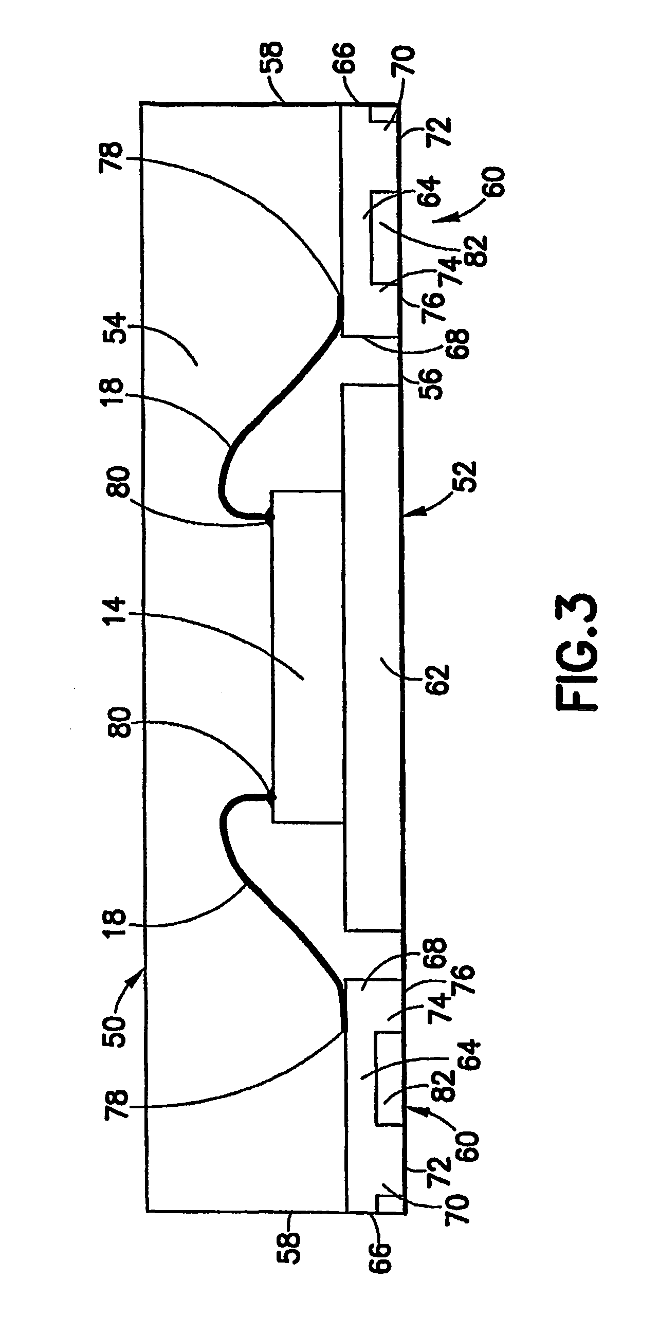
[0052]Referring to FIG. 3, a cross-sectional view of a quad, no-lead, wirebonded semiconductor device package 50 is shown. The semiconductor device package 50 includes a semiconductor device (die) 14 and a lead frame 52 covered by a molding compound 54, which forms a portion of outer faces 56 and 58 of the package 50. The lead frame 52 includes a plurality of leads 60 and a die pad 62 disposed between the leads 60. Each of the leads 60 includes an interposer 64 having one end 66 disposed proximate an outer face 58 of the package 50 and another end 68 disposed proximate the die 14. Extending from each interposer 64 proximate the end 66 is a board connecting post 70, which has a free end 72 that terminates at the package face 56. Extending from each interposer 64 proximate the opposite end 68 is a support post 74, which is spaced apart from the board connecting post 70 and has a free end 76 that terminates at the package face 56. Each of the leads 60 includes a bond site 78 formed on ...


PUM


Abstract

A lead frame (52, 100, 112) for a semiconductor device (die) package (50, 102, 110) is described. Each of the leads (60) in the lead frame (52, 100, 112) includes an interposer (64) having one end (66) disposed proximate the outer face (58) of the package (50, 102, 110) and another end (68) disposed proximate the die (14). Extending from opposite ends of the interposer (64) are a board connecting post (70) and a support post (74). A bond site (78) is formed on a surface of the interposer (64) opposite the support post (74). Each of the leads (60) is electrically connected to an associated input / output (I / O) pad (80) on the die (14) via wirebonding, tape bonding, or flip-chip attachment to the bond site (78). Where wirebonding is used, a wire electrically connecting the I / O pad (80) to the bond site (78) may be wedge bonded to both the I / O pad (80) and the bond site (78). The support post (74) provides support to the end (68) of the interposer (64) during the bonding and coating processes.(FIG. 3).

Description

CROSS-REFERENCE TO RELATED APPLICATION[0001]This application claims the benefit of U.S. Provisional Patent Application No. 60 / 494,982, filed Aug. 14, 2003, which is incorporated by reference herein in its entirety.BACKGROUND OF THE INENTION[0002]1. Field of the Invention[0003]This invention relates to semiconductor device packages. More particularly, this invention relates to lead frame based semiconductor device packages and methods for manufacturing lead frame based semiconductor device packages.[0004]2. Description of the Related Art[0005]In lead frame based semiconductor device packages, electrical signals are transmitted between at least one semiconductor device (die) and external circuitry, such as a printed circuit board, by an electrically conductive lead frame. The lead frame includes a number of leads, each having an inner lead end and an opposing outer lead end. The inner lead end is electrically connected to input / output (I / O) pads on the die, and the outer lead end prov...

Claims


Application Information

Patent Timeline
Patent Type & Authority Patents(United States)
IPC IPC(8): H01L21/00H01L23/48H01L
CPCH01L21/4832H01L23/3107H01L23/3114H01L23/49548H01L24/48H01L24/78H01L24/85H01L24/97H01L21/6835H01L2224/85099H01L24/45H01L24/81H01L24/86H01L2221/68377H01L2224/16245H01L2224/32245H01L2224/45124H01L2224/45144H01L2224/48091H01L2224/48227H01L2224/48247H01L2224/48455H01L2224/48465H01L2224/48472H01L2224/48599H01L2224/48699H01L2224/49171H01L2224/73265H01L2224/78302H01L2224/78313H01L2224/81801H01L2224/85001H01L2224/85205H01L2224/97H01L2924/01005H01L2924/01006H01L2924/01013H01L2924/01014H01L2924/01015H01L2924/01027H01L2924/01029H01L2924/01033H01L2924/0105H01L2924/01074H01L2924/01078H01L2924/01079H01L2924/01082H01L2924/014H01L2924/14H01L2924/15311H01L2224/78318H01L24/49H01L2924/01023H01L2924/12041H01L2924/00014H01L2224/45139H01L2224/85H01L2924/00012H01L2924/00H01L2224/45015H01L2924/181H01L2224/85203H01L2224/05599H01L2224/85399H01L24/73H01L2224/50H01L2224/86H01L2924/18301H01L2924/00015H01L23/48
Inventor ISLAM, SHAFIDULLAU, DANIEL K.SAN ANTONIO, ROMARICO S.SUBAGIO, ANANGMCKERREGHAN, MICHAEL H.LITILIT, EDMUNDA G-O.
Owner UNISEM M BERHAD
Why Eureka
Try Eureka