Integrated circuit package

a technology of integrated circuits and circuits, applied in the direction of semiconductor devices, semiconductor/solid-state device details, electrical apparatus, etc., to achieve the effect of reducing the number of external terminals, high i/o bus width, and high frequency memory components

Active Publication Date: 2009-07-21
MEMORY TECHNOLOGIES LLC
View PDF6 Cites 3 Cited by
  • Summary
  • Abstract
  • Description
  • Claims
  • Application Information

AI Technical Summary

Benefits of technology

[0009]Another object of the present invention is to provide the usage of high I / O bus width and high frequency memory components. The novel features of the flash memory I / O bus enables the usage of either NOR or NAND memory with unchanged device pin layout. The flash memory I / O bus provides a reduced number of external terminals compared to I / O buses having separate pins for the various flash memory types.
[0010]Another object of the present invention is to reduce the number of the pins or the external terminals of the package, the ASIC IC package in particular. Due to a limited number of available space and external terminals, solder balls in particular, the usage of pins and the number of pins is critical in POP devices in particular. The flash memory I / O bus or interface uses shared pins for the NOR and NAND type memories for reducing the amount of pins used exclusively for either one of the types.
[0011]Another object of the present invention is to provide an optimized I / O bus or interface for a 32-bit DDR SDRAM memory with either a NAND type or NOR type flash memory. The interface multiplexes NAND and NOR memory signals for providing a reduced I / O bus width for the package, and a reduced external terminal or pin count between the upper memory IC package and the lower ASIC IC package in particular. The multiplexed interface provides support for both NAND and NOR type flash memories with a minimum external terminal count, thereby enabling the choice between the NAND type or NOR type according to the requirements of the application or particular hardware.
[0013]Another object of the present invention is to provide an optimized signal placement of the DDR SDRAM I / O bus for reduced signal interference.

Problems solved by technology

Due to a limited number of available space and external terminals, solder balls in particular, the usage of pins and the number of pins is critical in POP devices in particular.

Method used


Image

  • Integrated circuit package
  • Integrated circuit package
  • Integrated circuit package

Examples


Embodiment Construction

[0021]Embodiments of the present invention will be described more specifically with reference to the accompanying drawings. In all the drawings illustrating the embodiments of the present invention, like elements having the same function will be identified by like reference numerals.

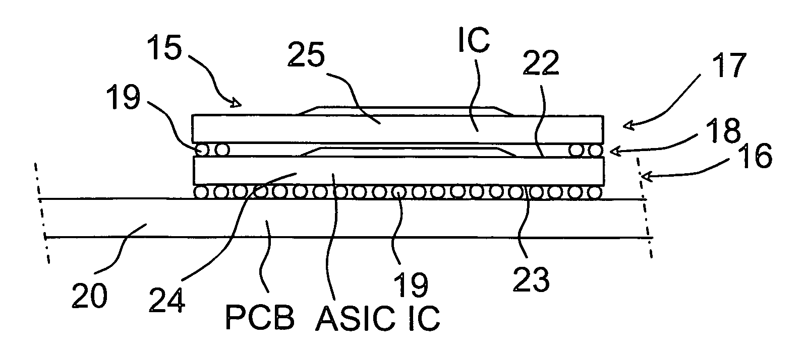
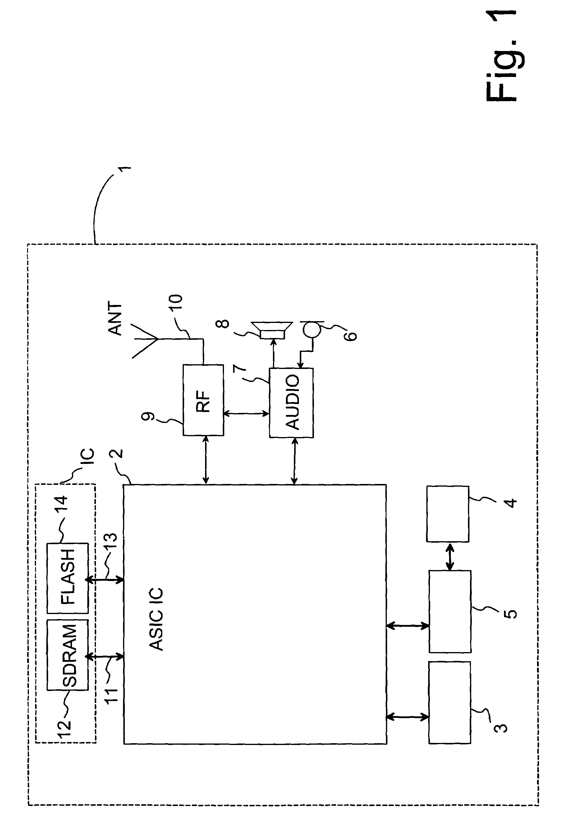
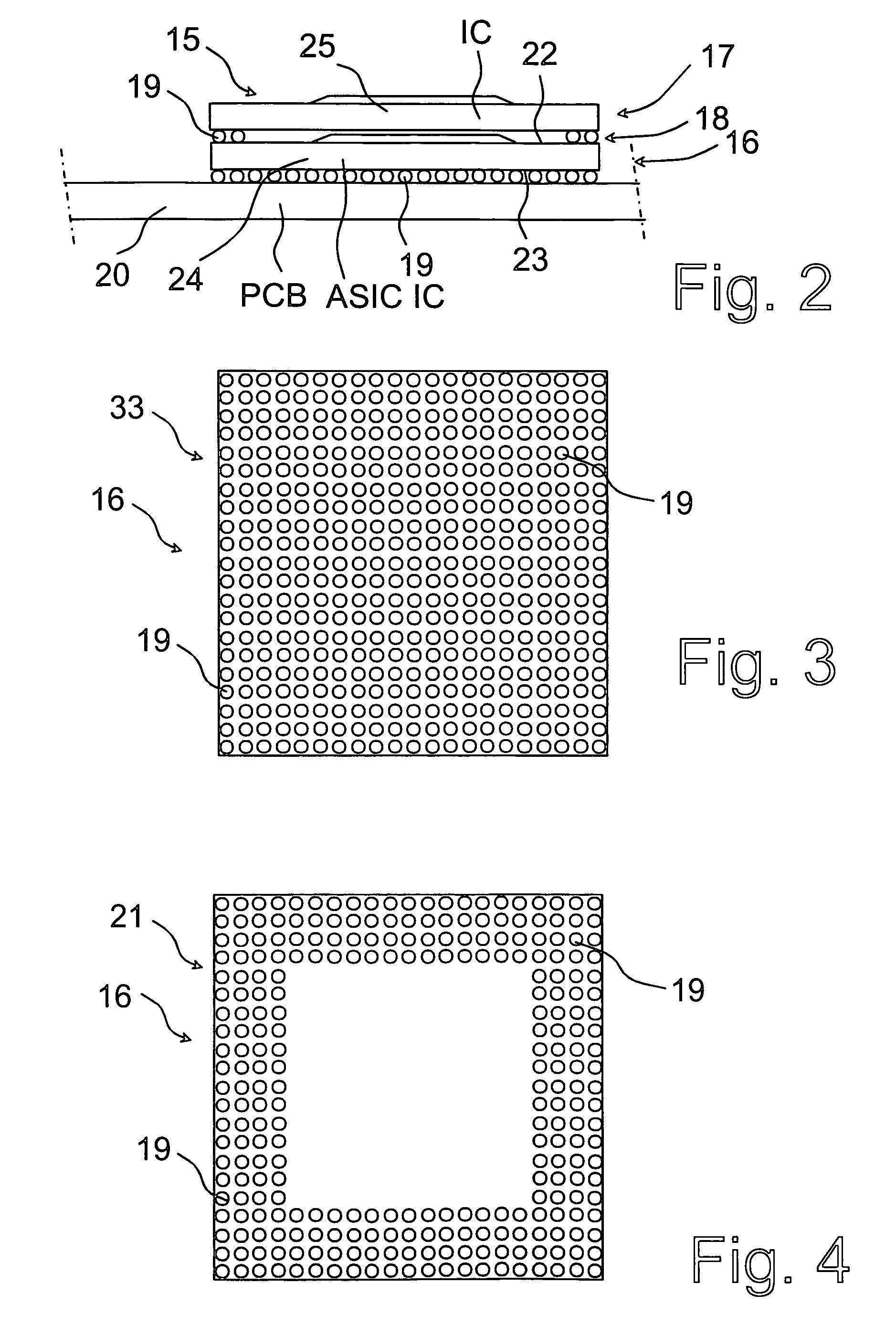
[0022]FIG. 1 is a simplified block diagram showing in one embodiment of the invention a mobile device 1 in which the invention is applied. The mobile device 1 functions in a way known as such. The mobile device 1, a mobile communication device or a mobile phone in particular, is a communication device comprising data processing functions and mobile station functions. Functions of the mobile device 1 are implemented in an ASIC IC 2. The ASIC IC 2 comprises e.g. a micro processing unit (MPU) being a universal RISC processor (Reduced Instruction Set Computer) and having cache memory. Furthermore, the ASIC IC 2 comprises a digital signal processor (DSP) for implementing signal processing functions. The ASIC ...


PUM


Abstract

An integrated circuit package comprising: an substrate having a first main surface and a second main surface which are opposite to each other; a first plurality of external terminals disposed on the first main surface of said interconnection substrate; and a second plurality of external terminals disposed on the second main surface of said interconnection substrate; wherein said second plurality of external terminals comprises a predefined selection of shared external terminals defining a first interface for an integrated circuit memory package having type NAND or type NOR memory.

Description

BACKGROUND OF THE INVENTION[0001]The present invention relates to the field of electronic interconnection structures and IC packaging technology.[0002]Current integrated circuit (IC) chip packaging technologies commonly rely on an interconnection substrate containing circuitry to serve as an interconnection base. The interconnection base redistributes the I / O (input / output) terminals or external terminals of the IC to a more optimized contact spacing for making an interconnection between I / O terminals or external terminals of the other parts of assembly. An example of the assembly is when the IC package is mounted on and interconnected to a printed circuit board (PCB). The interconnection between the IC chip or die and the chosen package is normally accomplished using wire bonding, which connects the chip terminals to terminals on the package by thin wires. Alternatively, the chip terminals are interconnected to the IC package substrate by means of metal bumps, solder balls or condu...

Claims


Application Information

Patent Timeline
Patent Type & Authority Patents(United States)
IPC IPC(8): H01L23/06
CPCH01L23/50H01L25/105H01L25/18H01L2924/15311H01L2924/15331H01L2924/0002H01L2225/1023H01L2225/1058H01L2924/00
Inventor JAURIMO, SAKUSIPPOLA, SAKARI
Owner MEMORY TECHNOLOGIES LLC
Why Eureka
Try Eureka