Laser mask and crystallization method using the same
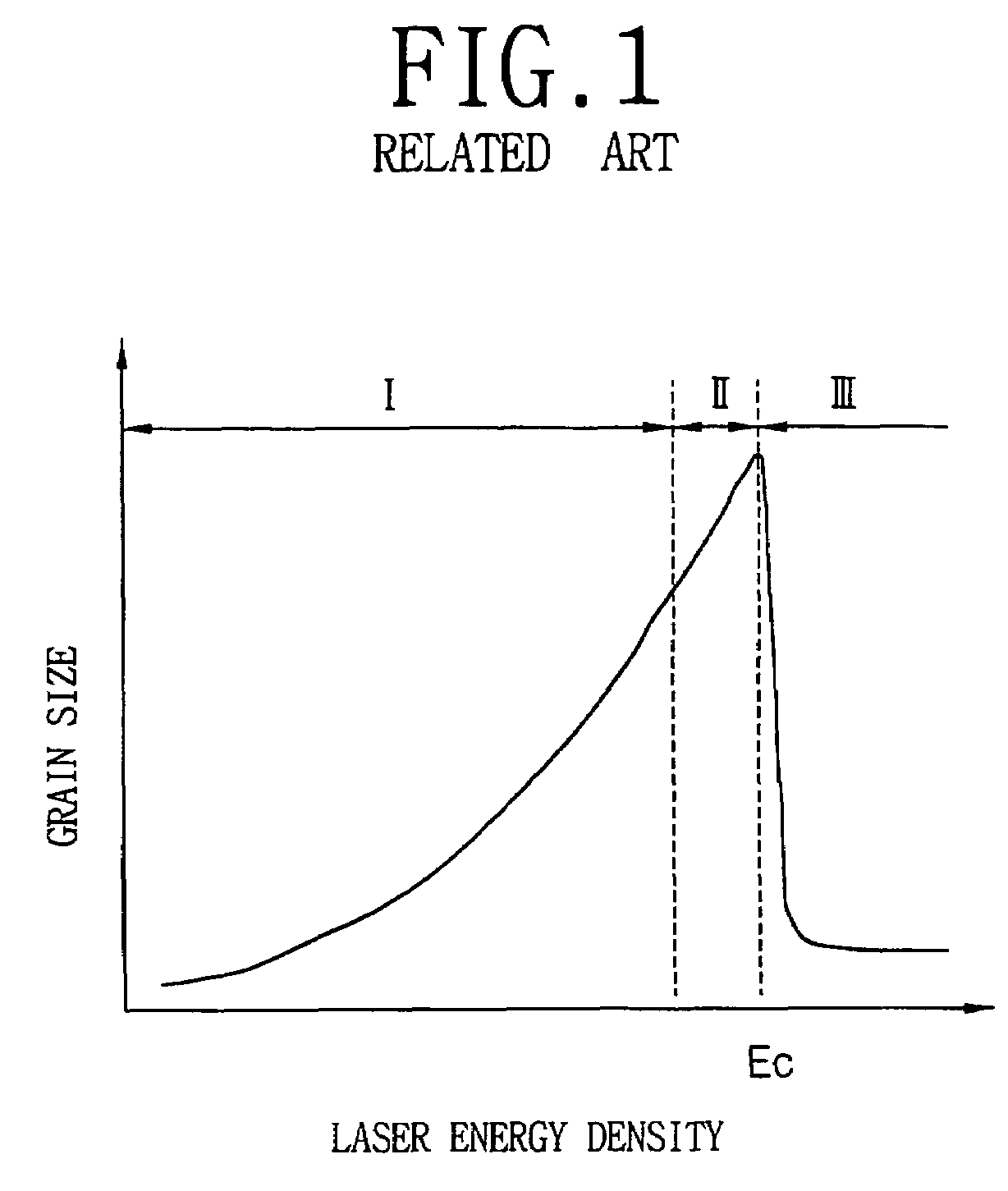
a laser mask and crystallization method technology, applied in the field of laser masks and crystallization methods, can solve the problems of non-uniform characteristics of devices manufactured from crystallized thin films, defects that affect the performance of tfts next to gray boundaries, and limit the use of amorphous silicon tfts with electrical mobility 1 cm, so as to reduce overlap and reduce the effect of diffraction
- Summary
- Abstract
- Description
- Claims
- Application Information
AI Technical Summary
Benefits of technology
Problems solved by technology
Method used
Image

Examples
first embodiment
[0118]FIG. 11A shows a sectional view illustrating a laser mask according to the invention. An improved laser mask having a novel shape of the edges of the slit pattern is illustrated.
[0119]FIG. 11A shows a laser mask 470 that has transmitting regions 473 with concave edges that transmit light and a blocking region 474 that blocks light.
[0120]The mask 470 blocks all of the laser beams incident on the blocking region 474 excluding that transmitting regions 473 of the slit pattern 475 formed in the center thereof. The mask 470 may be formed of aluminum or aluminum based alloy that effectively blocks laser beams and that has high reflectance. However, the invention is not restricted to aluminum, and any suitable mask material can be used. Also, organic materials can be used to form the mask.
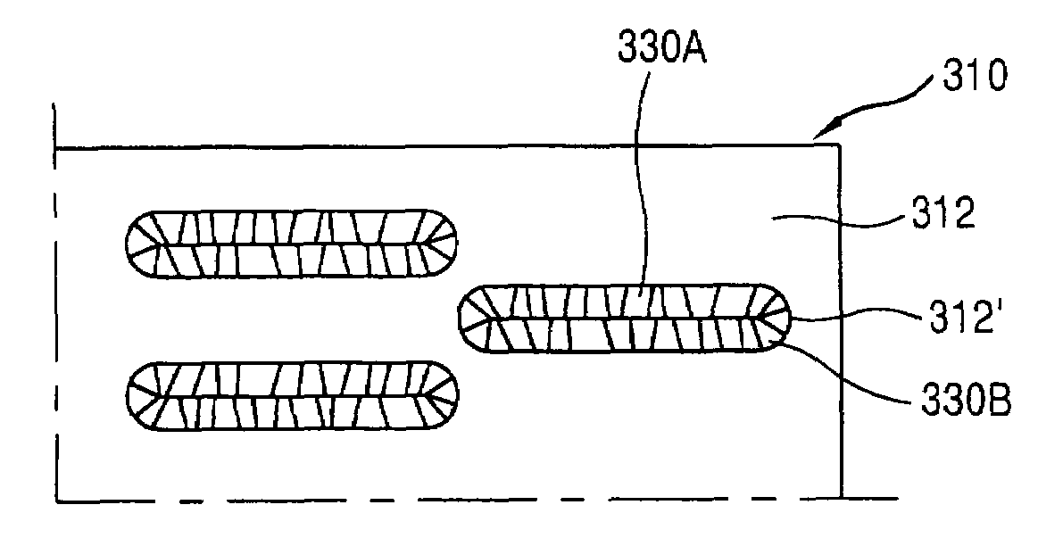
[0121]FIG. 11B shows a plan view schematically illustrating the crystallization shape of the silicon thin film crystallized using the mask illustrated in FIG. 11A. As illustrated in FIG. 11B, the si...
second embodiment
[0129]FIG. 14 shows a plan view illustrating a laser mask according to the invention. A two-block laser mask capable of performing two-shot horizontal crystallization by a single scan in the X-axis direction is illustrated.
[0130]As illustrated in FIG. 14, a laser mask 570 includes a slit pattern 575 in which offset transmitting regions 573 have concave edges with predetermined width and length.
[0131]The laser mask 570 is a two-block laser mask that has transmitting regions 573 with concave edges that transmit light. A blocking region 574 blocks light such that two transmitting regions 573 are arranged on the left side of the laser mask 570, and one transmitting region 573 is arranged on the right side of the laser mask 570 to offset each other.
[0132]A process of crystallizing a silicon thin film using the laser mask 570 of the above-described structure will be described below.
[0133]FIGS. 15A to 15C show plan views sequentially illustrating a process of crystallizing a silicon thin f...
PUM
| Property | Measurement | Unit |
|---|---|---|
| driving voltage | aaaaa | aaaaa |
| driving voltage | aaaaa | aaaaa |
| melting temperature | aaaaa | aaaaa |
Abstract
Description
Claims
Application Information
 - R&D
- Intellectual Property
- Life Sciences
- Materials
- Tech Scout
- Unparalleled Data Quality
- Higher Quality Content
- 60% Fewer Hallucinations
Browse by: Latest US Patents, China's latest patents, Technical Efficacy Thesaurus, Application Domain, Technology Topic, Popular Technical Reports.
© 2025 PatSnap. All rights reserved.Legal|Privacy policy|Modern Slavery Act Transparency Statement|Sitemap|About US| Contact US: help@patsnap.com