Method of forming conducting nanowires

a nanowire and conducting technology, applied in the field of nanowire assembly, can solve the problem of difficult contact with an unsupported nanowir

Inactive Publication Date: 2009-08-04
TRINITY COLLEGE DUBLIN
View PDF10 Cites 7 Cited by
  • Summary
  • Abstract
  • Description
  • Claims
  • Application Information

AI Technical Summary

Benefits of technology

[0033]It is a considerable advantage of the present invention that the nanowires are now formed positioned on the substrate in contrast to being unsupported and additionally the nanowires are advantageously present on the substrate in a planar fashion. It is also possible in accordance with the invention to provide the nanowires so that they are positioned on the substrate in a preferential orientation along a given direction of the substrate surface. This is yet another significant advantage of the invention.
[0034]It will be understood that the method of the invention enables the formation of an array of conducting or semi-conducting nanowires wherein the separation between the nanowires and the cross-sectional dimensions of the nanowires can be controlled. Preferably, the separation between the nanowires is in the range from approximately 0.2 nm to approximately 50 nm. Ideally, the cross-sectional dimensions of the nanowires is in the range of from approximately 1 nm to approximately 50 nm.
[0035]According to yet another aspect of the invention, a doped semiconductor material may be deposited to form the dopant nanowires. Preferably, a thin film of doped semiconductor is formed on the vicinal surface of the substrate. If a doped semiconductor material is used in this manner, it will be understood that there may be no need for the deposition of an over layer and a subsequent annealing step. The nanowires will form directly after deposition of the doped semiconductor.
[0036]According to another embodiment of this aspect of the invention, a layer (fractional or otherwise) of dopant material is deposited to form nanostripes. Preferably, the layer of dopant material is deposited at a non-glancing angle to result in the entire surface or part of the surface of the substrate being covered by the dopant. The surface is then exposed to energized ion beam etching of the dopant material at a shallow angle with respect to the surface to remove the dopant material from some parts of the atomic terraces to form the nanostripes. Preferably, the energized ion beam is collimated and directed at an angle that is substantially the same as the miscut angle of the substrate. The energized ion beam may be Argon ions accelerated to the energy of 20 KeV or 200 KeV.
[0037]An alternative embodiment of this aspect of the invention involves the deposition of a layer (fractional or otherwise) of dopant material to form the nanostripes. Preferably, the layer of dopant material is deposited at a non-glancing angle to result in the entire surface or most of the surface of the substrate being covered by the dopant. The surface is exposed to a collimated beam of chemically reactive species which reacts with the substrate and etches the dopant material away to form the nanostripes. Preferably, the beam is collimated and directed at a shallow angle with respect to the surface. Preferably, the angle is substantially the same as the miscut angle of the substrate. Preferably, the chemically reactive species is a chemically reactive plasma that reacts with Si for example and turns it into SiH4 or another gas that is easily removed.
[0038]According to these alternative embodiments of the invention, some areas of the atomic terrace are not exposed to the beam or are exposed to it to a much smaller extent than other areas. These areas form the nanostripes. The width of the nanowires is controlled by the ability to control the angle of the beam with respect to the atomic terraces of the substrate.

Problems solved by technology

In practice this means that the nanowire or an array of nanowires should be positioned on a flat substrate, as making contacts to an unsupported nanowire is difficult.

Method used


Image

  • Method of forming conducting nanowires
  • Method of forming conducting nanowires
  • Method of forming conducting nanowires

Examples


Embodiment Construction

[0120]The invention can be more clearly understood from the following description of some embodiments thereof, given by way of example only with reference to accompanying drawings in which:

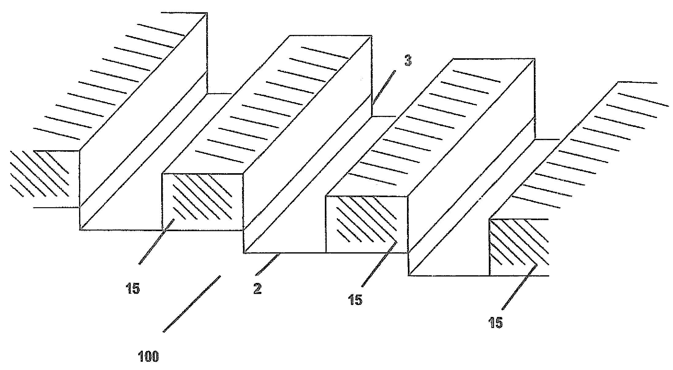
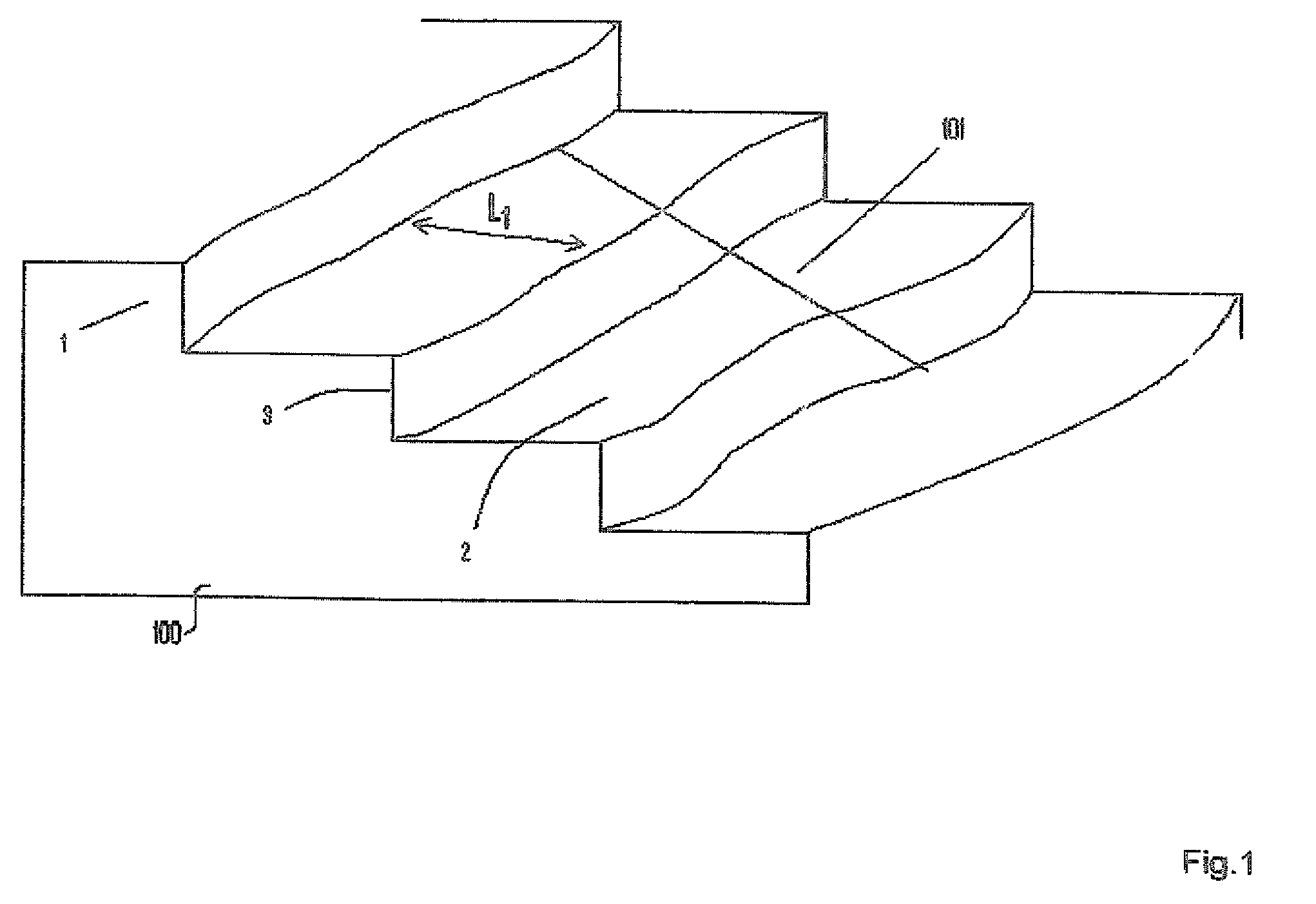
[0121]FIG. 1. is a perspective view of a typical vicinal surface of a substrate;

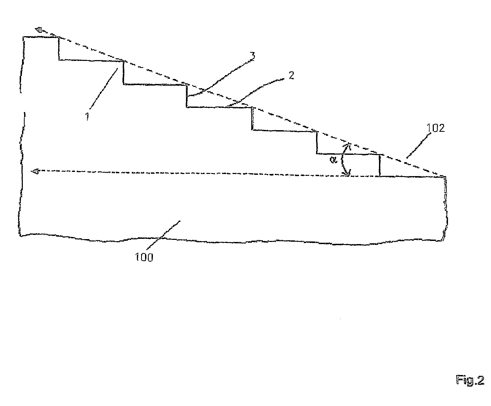
[0122]FIG. 2 is a cross-section perpendicular to the terrace steps of the vicinal substrate;

[0123]FIG. 3 is a schematic representation of adatoms of a layer deposited on the substrate before they arrive at equilibrium positions. Adatoms located at the outer and inner edges of a terrace step are shown;

[0124]FIG. 4 shows formation of the closed fractional layer at the inner edges of terrace steps;

[0125]FIG. 5 is a perspective view of a closed fractional layer formed at the inner edges of the terrace steps;

[0126]FIG. 6 is a diagrammatic representation of portion of another array of nanowires during its formation with a closed fractional layer at the outer edges of the terrace steps;

[0127]FIG. 7 is a diagrammatic represent...


PUM

PropertyMeasurementUnit
lengthaaaaaaaaaa
sizeaaaaaaaaaa
diameteraaaaaaaaaa

Abstract

A method of preparing an array of conducting or semi-conducting nanowires may include forming a vicinal surface of stepped atomic terraces on a substrate, and depositing a fractional layer of dopant material to form nanostripes having a width less than the width of the atomic terraces. Diffusion of the atoms of the dopant nanostripes into the substrate may form the nanowires.

Description

INTRODUCTION[0001]The present invention relates to a nanowire assembly and in particular to a method for preparing such a nanowire assembly. It further relates to various electronic devices, including field effect transistors, comprising the nanowire assembly.[0002]During the recent years there has been a massive increase in research effort on nanoscale conducting objects. Most commonly the attention in this area is paid to nanowires. In this specification, the term “conducting nanowire” or more simply “nanowire” is defined generally as an elongated object in which both of its orthogonal cross-sectional dimensions are in the nanoscale range: e.g. 0.2-20 nm and that is capable of transferring charge along its length. Both terms “nanowires” and “conducting nanowires” are used interchangeably in this specification. It is important to stress that both of the cross sectional dimensions must be in this range, not only one of them. Those skilled in the art will readily appreciate that if t...

Claims


Application Information

Patent Timeline
Patent Type & Authority Patents(United States)
IPC IPC(8): H01L21/44
CPCH01L21/76838B82Y10/00
Inventor FERNANDEZ-CEBALLOS, SERGIOMANAI, GIUSEPPESHVETS, IGOR VASILIEVICH
Owner TRINITY COLLEGE DUBLIN
Why Eureka
Try Eureka