

Microfluidic device and method of manufacturing the same
a microfluidic device and microfluidic technology, which is applied in the field of manufacturing a microfluidic device, can solve the problems of difficult uniform binding of biomaterials to desired regions, easy damage to the organic functional group of the coupling agent attached to the si substrate for biomaterial introduction, and increase in the degree of dispersion of the coupling agent in the microchannel
- Summary
- Abstract
- Description
- Claims
- Application Information
AI Technical Summary
Benefits of technology
Problems solved by technology
Method used
Image

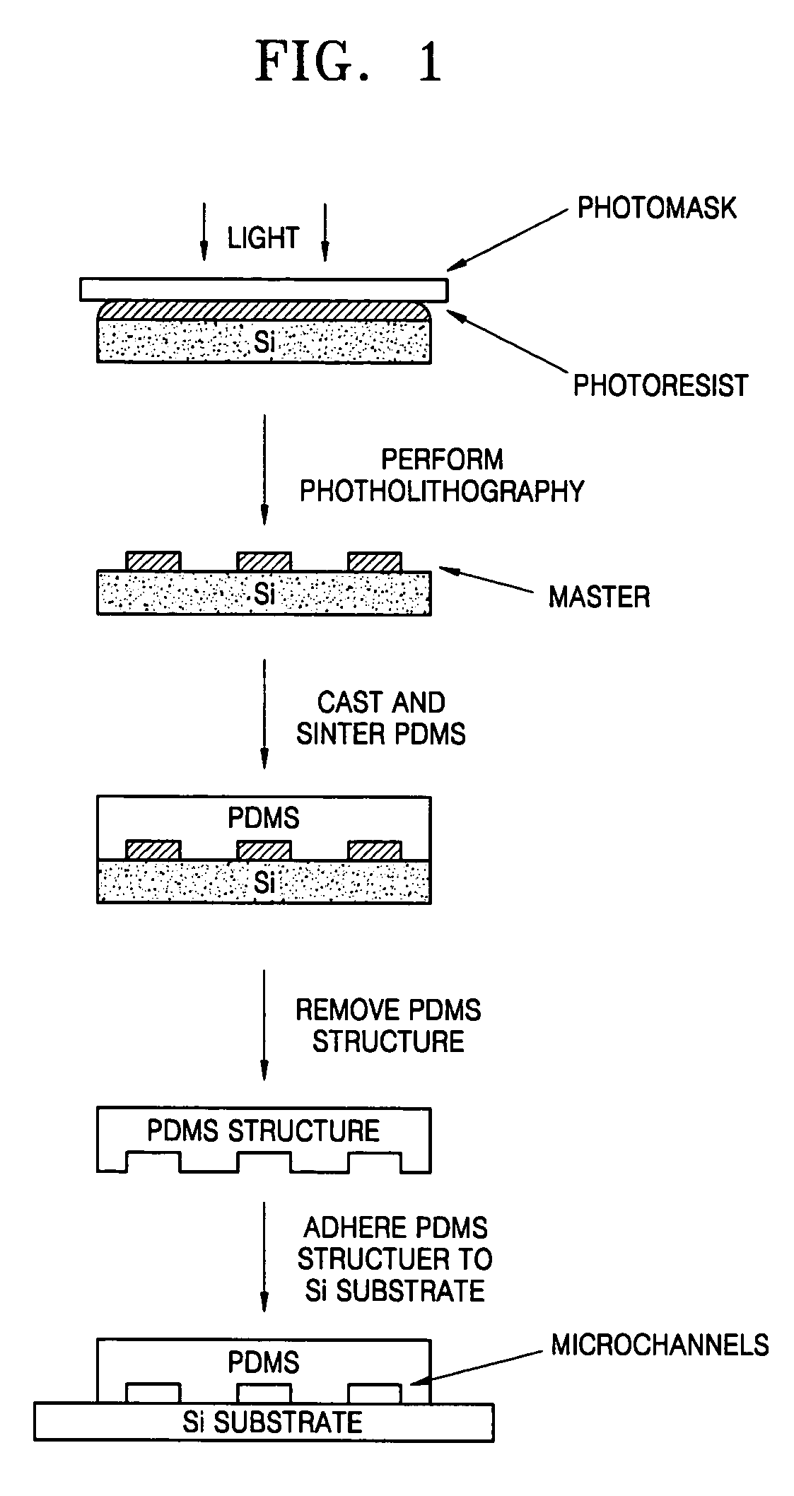
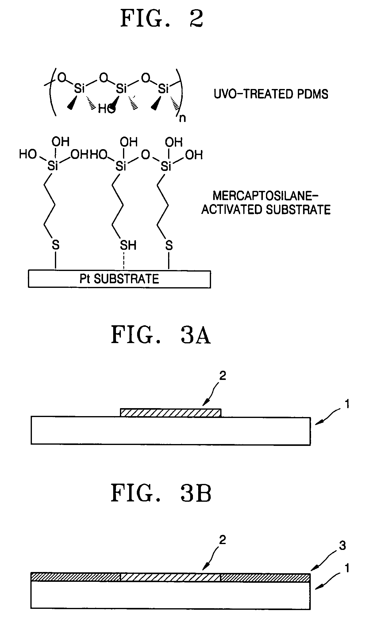
Examples
example 1
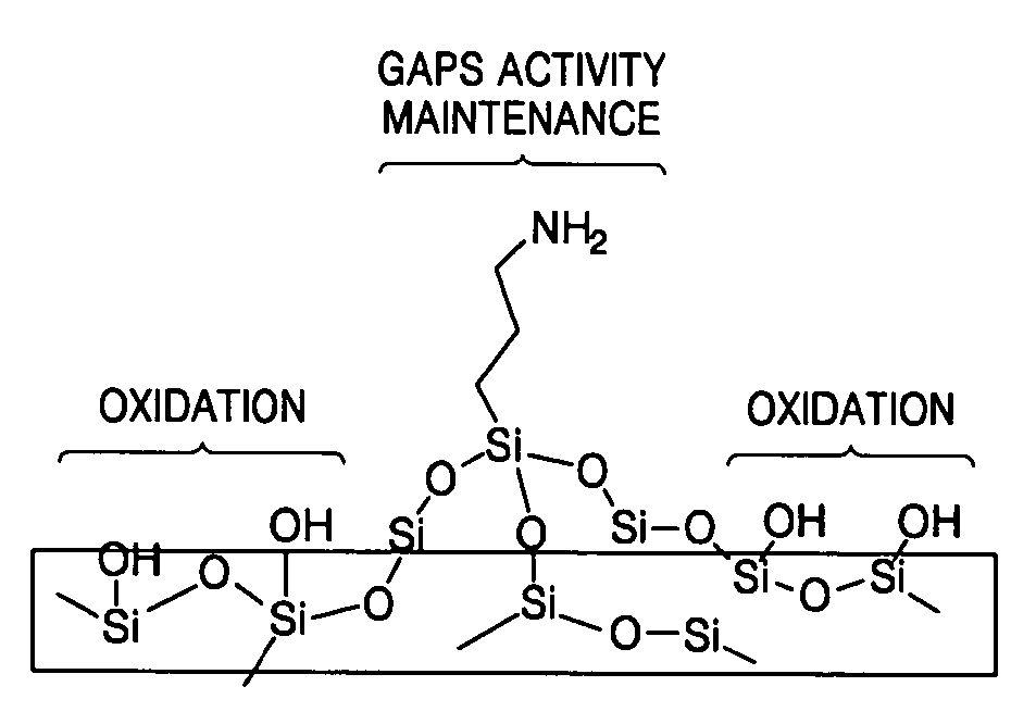
[0073](1) Formation of Oxide Film on Wafer
[0074]An oxide film was formed to a thickness of 1,000 Å on a silicon wafer by thermal oxidation using Furnace SVF-200 (Celtron). The formation of the oxide film and all the following experiments were performed in a cleanroom-class 1000 with few or no dust particles.
[0075]The thickness of the oxide film was measured using NANOSPEC Model AFT 200 (NANOMETTICS). The NANOSPEC Model AFT 200 is a machine that measures the thickness of an oxide film using the principle that when light is incident in a silicon wafer, some light is reflected from the oxide film and some light passes through the oxide film and is then reflected from the silicon wafer. The thickness of the oxide film is measured using a phase difference between the light reflected from the oxide film and the light reflected from the silicon wafer. In the Example, the silicon wafer was placed on a sample stage of the NANOSPEC and the thickness of the oxide film at six points on the sili...
example 2
[0099]A microfluidic device was manufactured in the same manner as in Example 1 except that a 30% (w / v) hydrogen peroxide aqueous solution was used to selectively oxidize coupling agent-free regions of a silicon wafer.
example 3
[0100]A microfluidic device was manufactured in the same manner as in Example 1 except that a 2.38% (w / v) tetramethylammonium hydroxide aqueous solution was used to selectively oxidize coupling agent-free regions of a silicon wafer.
PUM
| Property | Measurement | Unit |
|---|---|---|
| temperature | aaaaa | aaaaa |
| energy | aaaaa | aaaaa |
| pressure | aaaaa | aaaaa |
Abstract
Description
Claims
Application Information