Atomic layer deposition method for depositing a layer

a layer and atomic layer technology, applied in chemical vapor deposition coatings, electrical devices, coatings, etc., can solve the problems of poor interface quality, difficult control of interface quality, poor chemical and electrical properties, etc., and achieve the effect of improving the chemical and electrical characteristics of the deposited layer

Active Publication Date: 2009-08-25
INTERUNIVERSITAIR MICRO ELECTRONICS CENT (IMEC VZW)
View PDF6 Cites 326 Cited by
  • Summary
  • Abstract
  • Description
  • Claims
  • Application Information

AI Technical Summary

Benefits of technology

[0010]The present invention aims to provide an ALD method to improve the chemical and electrical characteristics of the deposited layer.

Problems solved by technology

Since for ALD processes the deposition is very temperature sensitive, this control of the interface quality is very challenging.
However, data from electrical evaluation of devices with high-k grown with a standard ALD process consequent to these surface preparation methods indicates poor interface quality.
At lower temperature the silicon surface has a significantly higher concentration of surface hydroxyls than under the conventional deposition temperature of 300° C. However, the lower temperature has the negative side effect of not driving the ALD reaction cycle to completion.

Method used


Image

  • Atomic layer deposition method for depositing a layer
  • Atomic layer deposition method for depositing a layer
  • Atomic layer deposition method for depositing a layer

Examples


example 1

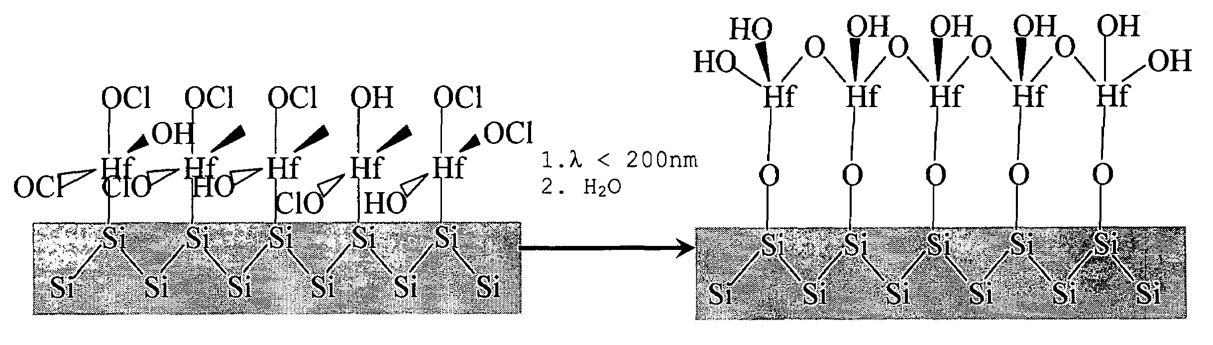
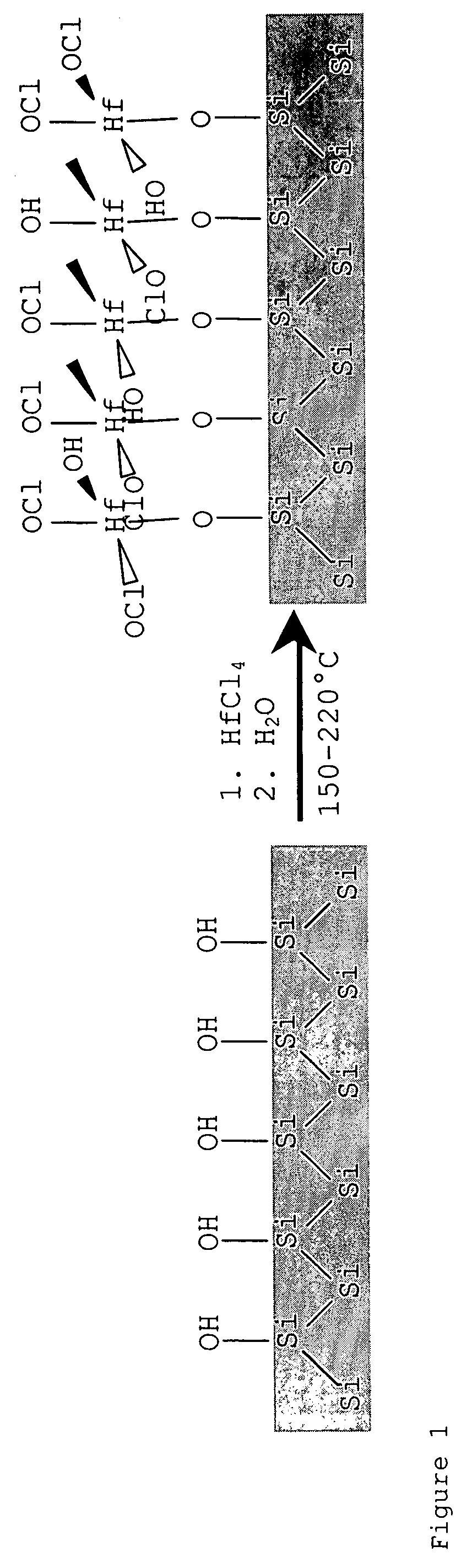
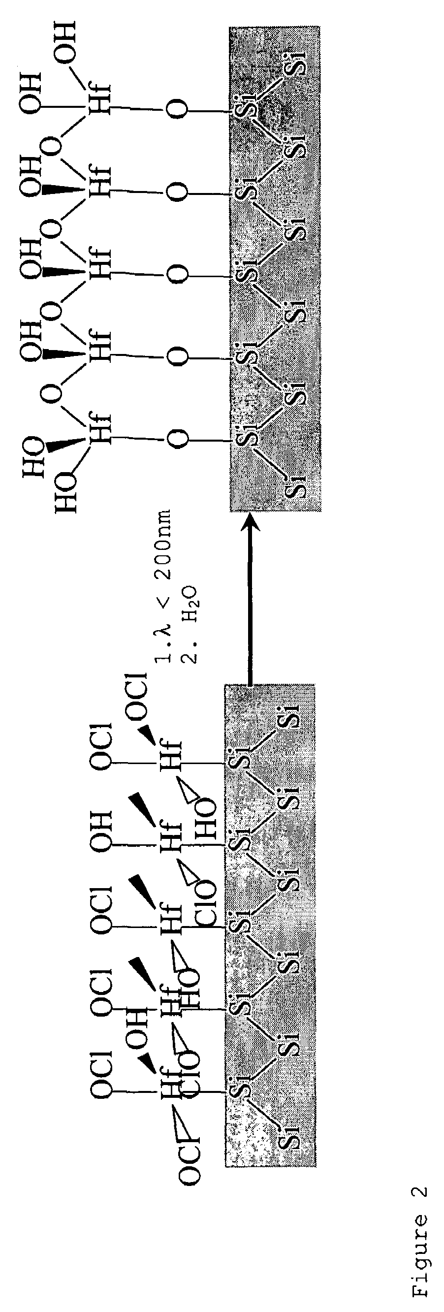
[0099]As a first example of the invention, the ALD of hafnium chloride is performed at lower temperatures (than usually performed), in the range of 150° C.-220° C. (FIG. 1).

[0100]At these temperatures, the Si surface has a significantly higher concentration of surface hydroxyls than under the conventional deposition temperature of 300° C.

[0101]However, the lower temperature has the negative side effect of not driving the HfCl4 reaction to completion.

[0102]The resulting species has some concentration of—OCl termination of the Hf instead of the more desirable—OH termination.

[0103]So, although the growth rate of the ALD can be nearly a monolayer (˜0.2 nm) per cycle, the defects introduced by the OCl terminations will make for a poor quality layer.

[0104]Additionally, it is difficult to remove the residual Cl out of the layers through post deposition anneals.

[0105]When treating (exposing) the semiconductor substrate with UV in the first one to five cycles, dissociation of HfCl4 is increa...

example 2

[0112]As a second example of the invention, the ALD starts with the conventional process at 300° C. but in this case the Si surface looks significantly different.

[0113]FIG. 3 shows a schematic of the Si surface at 300° C. One can clearly see the difference compared to the starting surface in FIG. 1.

[0114]With this high temperature, adjacent hydroxyls react as shown in FIG. 4, leaving few isolated OH groups.

[0115]This dramatically reduces the surface coverage in the first few cycles of the ALD process.

[0116]In FIG. 5A-C, possible starting surface compositions following 1-3 cycles of HfCl4 and H2O are illustrated. After UV treatment (FIG. 5D) the surface coverage is increased dramatically.

example 3

[0117]An ALD deposition is done on a silicon semiconductor substrate, starting from HCl4 as first precursor and H2O as second precursor.

[0118]Between the HCl4 pulse and the H2O pulse an inert atmosphere is provided by purging the reactor with nitrogen.

[0119]A nitrogen purge is also done after the H2O pulse.

[0120]A spot of about 40 mm width on the silicon substrate is then exposed to a 172 nm UV irradiation during one of the two nitrogen purges.

[0121]In FIG. 6, the difference in layer thickness measured by ellipsometry between the substrate surface exposed to UV irradiation and the substrate surface not exposed to UV irradiation is shown.

[0122]The triangles (▴) show the layer thickness after 10 cycles of conventional ALD without UV exposure.

[0123]The dots (●) show the layer thickness after 10 cycles of conventional ALD deposition, followed by 3 min UV exposure as a post-deposition treatment.

[0124]The diamonds (♦) show the layer thickness after 10 cycles of ALD including in each cycle...


PUM

PropertyMeasurementUnit
wavelengthaaaaaaaaaa

Abstract

The invention is related to an ALD method for depositing a layer including the steps of a) providing a semiconductor substrate in a reactor; b) providing a pulse of a first precursor gas into the reactor; c) providing a pulse of a second precursor gas into the reactor; d) providing an inert atmosphere in the reactor; and e) repeating step b) through step d), wherein at least once during step d) the semiconductor substrate is exposed to UV irradiation.

Description

CROSS-REFERENCE TO RELATED APPLICATIONS[0001]This application claims the benefit under 35 U.S.C. § 119(e) of U.S. provisional application Ser. No. 60 / 698,331, filed Jul. 11, 2005, the disclosure of which is hereby incorporated by reference in its entirety and is hereby made a portion of this application.FIELD OF THE INVENTION[0002]The invention relates to an improved ALD method for depositing layers in the field of semiconductor processing. The invention also relates to a semiconductor device obtainable by a method according to the invention.BACKGROUND OF THE INVENTION[0003]Because in the field of electronics in general further downscaling of the semiconductor devices is always proceeding, deposition processes have to be developed that are able to deposit layers with a thickness control at atomic layer scale. One of these deposition techniques is Atomic Layer Deposition (ALD), often used for depositing dielectric layers.[0004]In order to achieve satisfying semiconductor device chara...

Claims


Application Information

Patent Timeline
Patent Type & Authority Patents(United States)
IPC IPC(8): H01L21/31H01L21/469
CPCC23C16/405C23C16/45536H01L21/3141C23C16/483C23C16/482H01L21/02205H01L21/0228H01L21/02181H01L21/0231
Inventor ZIMMERMAN, PAULCAYMAX, MATTYDE GENDT, STEFANDELABIE, ANNELIESRAGNARSSON, LARS-AKE
Owner INTERUNIVERSITAIR MICRO ELECTRONICS CENT (IMEC VZW)
Why Eureka
Try Eureka