Semiconductor integrated circuit

a technology of integrated circuits and semiconductors, applied in the field of semiconductor integrated circuits, can solve problems such as unsuitable integration, and achieve the effect of reducing the influence of quantizer spike noise on the input signal to the resonator

Active Publication Date: 2009-09-01
RENESAS ELECTRONICS CORP
View PDF2 Cites 37 Cited by
  • Summary
  • Abstract
  • Description
  • Claims
  • Application Information

AI Technical Summary

Benefits of technology

[0026]Therefore, the adder (Add) forms a feedforward path (Ffd) for supplying the analog input signal (Vin) to the input of the quantizer (95). Substantially only a quantization error of the difference between a digital output of the quantizer (95) with respect to the analog input signal (Vin) and the analog input signal (Vin) is supplied to the inside of the resonator (92, 94). The level of a signal formed by only the quantization error supplied to the inside of the resonator is lowered widely in comparison to the signal level obtained in the band pass ΔΣ modulator as shown in FIG. 2. Hence, the gain of the resonator can be made larger, and the equivalent input noise of the resonator can be reduced. Thus, a good S / N ratio can be achieved.
[0027]The inventors thus conceived a basic technical idea of the invention concerning an A / D converter constructed with a non-quadrature band pass ΔΣ modulator that a feedforward path for supplying an analog input signal to an input of a quantizer is provided and a quantization error is supplied to an input of a resonator, thereby reducing the level of an input signal of the resonator greatly. Now, it is noted that a non-quadrature band pass ΔΣ modulator associated with the invention is not affected by an overhead caused by an orthogonal mixer and the variation between two routes, which become problems for a band pass ΔΣ modulator of a quadrature type.
[0029]Further, it is described in Non-patent Document 6 that in a band pass (BP) ΔΣ modulator of a quadrature type, an analog input signal is directly supplied to an input of a quantizer. However, Non-patent Document 6 does not contain any description concerning a first half portion of the basic technical idea of the invention, i.e. a band pass (BP) ΔΣ modulator of a non-quadrature type. Also, in this document, the following descriptions are not contained. The first is that the level of an input signal to a resonator is lowered greatly and the gain of the resonator can be made higher. The second is that the equivalent input noise of the resonator is lowered, and therefore a good S / N ratio can be achieved.
[0030]Of the forms of a semiconductor integrated circuit disclosed therein, the effect offered by the preferred ones is as follows in brief. That is, the invention makes it possible to improve the S / N ratio of an A / D converter constructed with a band pass ΔΣ modulator.

Problems solved by technology

Super heterodyne receivers of a multi-stage type have a large number of passive elements, and therefore they are not suitable for integration.

Method used


Image

  • Semiconductor integrated circuit
  • Semiconductor integrated circuit
  • Semiconductor integrated circuit

Examples


Embodiment Construction

1. Summary of the Preferred Embodiments

[0042]First, the preferred embodiments of the invention disclosed therein will be described in brief outline. The reference numerals and characters of the drawings for making reference which are put here in parentheses only exemplarily show what the concepts of the constituent elements marked with the reference numerals and characters contain.

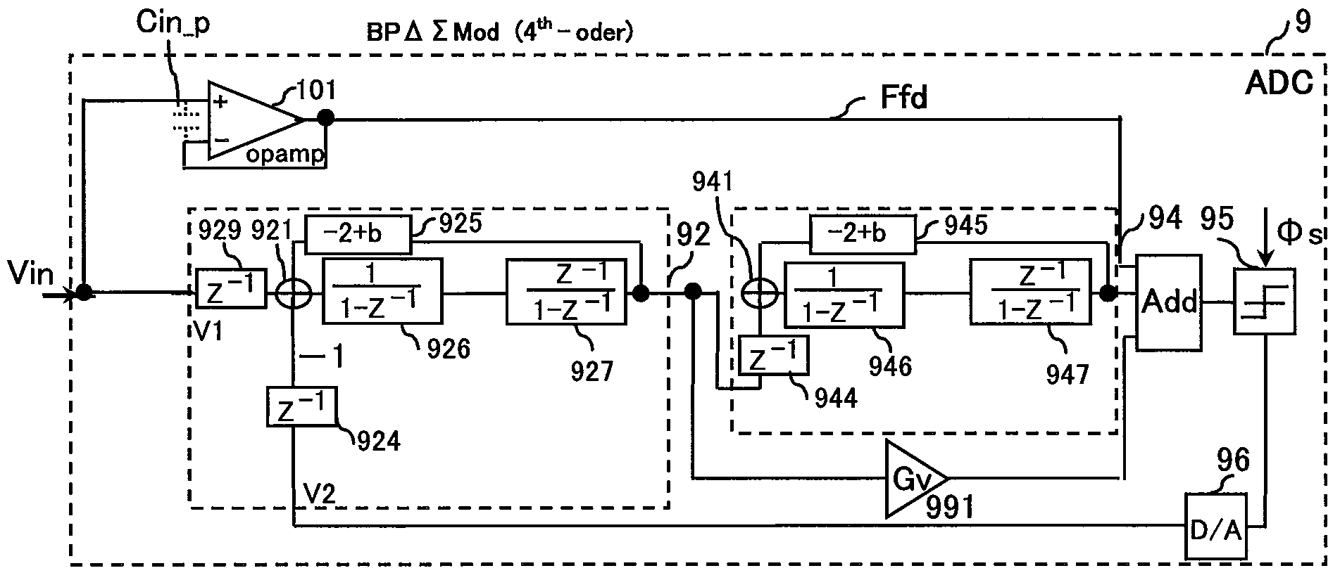
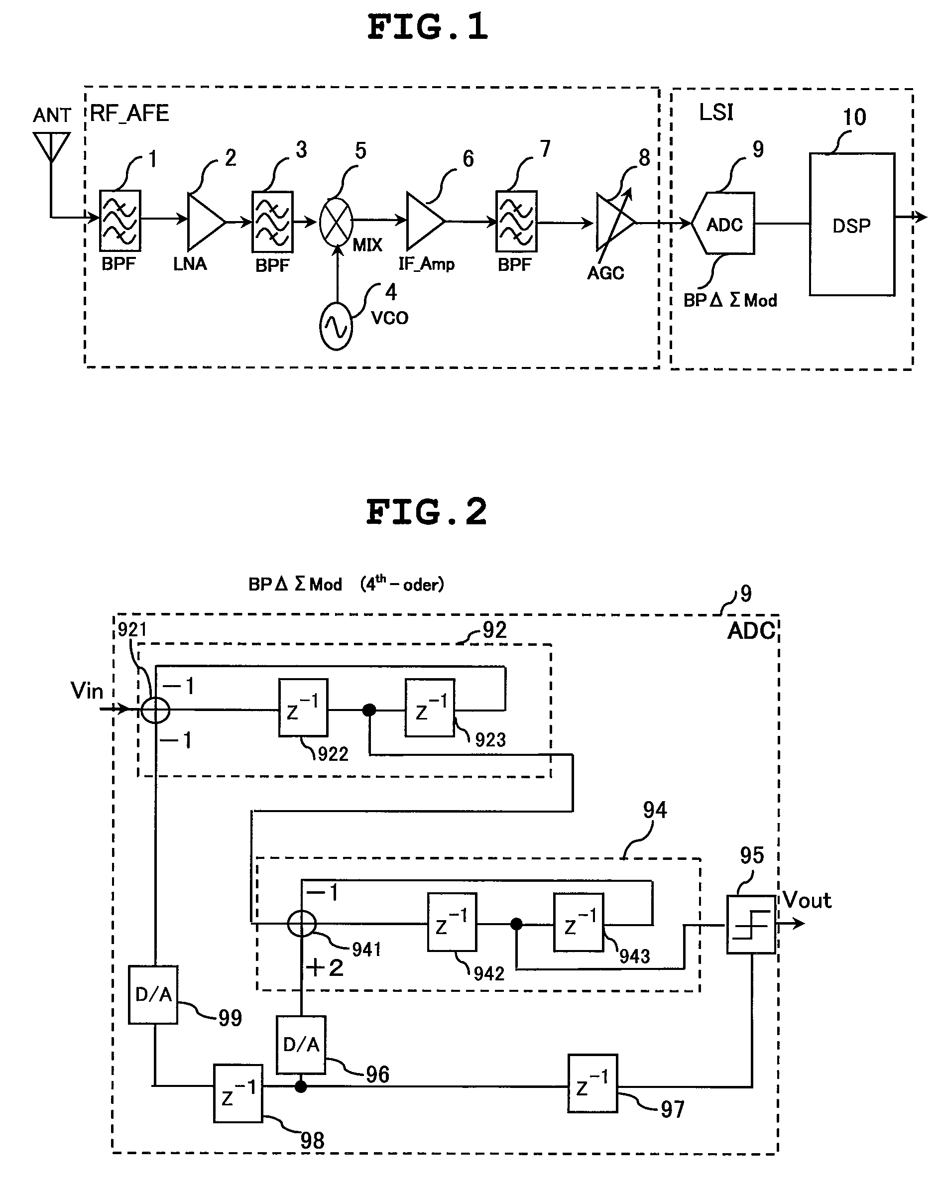
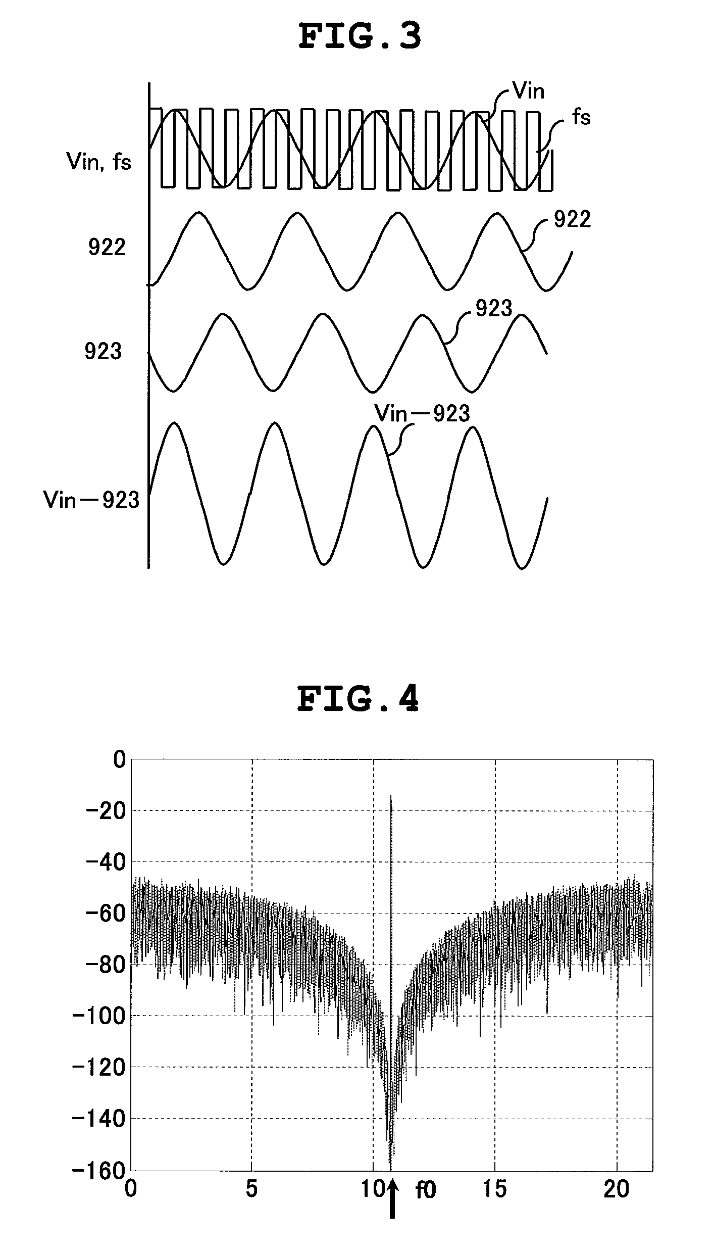
[0043][1] A semiconductor integrated circuit (LSI) according to a preferred embodiment of the invention includes an A / D converter (9) which is constructed with a non-quadrature band pass ΔΣ modulator (BPΔΣMod) and converts an analog input signal (Vin) into a digital output signal (Vout). The band pass ΔΣ modulator includes a resonator (92, 94) responding to the analog input signal to show a band-pass characteristic at a predetermined frequency (f0), and show an attenuation characteristic at a frequency different from the predetermined frequency. The band pass ΔΣ modulator includes a quantizer (95) to which...


PUM


Abstract

The A / D converter converting an analog input signal into a digital output signal is constructed with a band pass ΔΣ modulator. The band pass ΔΣ modulator includes: a resonator showing a band-pass characteristic at a predetermined frequency and an attenuation characteristic at another frequency; a quantizer; and a local D / A converter. A signal of difference between the analog input signal and a local analog signal of the local D / A converter is supplied to the resonator. The A / D converter further includes an adder for supplying the analog input signal to an input of the quantizer. In addition, signal transmission circuits for reducing the influence of spike noise of the quantizer on the input to the resonator are connected between an input of the adder and an input of resonator selectively. The A / D converter constructed with the band pass ΔΣ modulator is improved in S / N ratio.

Description

CLAIM OF PRIORITY[0001]The Present application claims priority from Japanese application JP 2007-006821 filed on Jan. 16, 2007, the content of which is hereby incorporated by reference into this application.FIELD OF THE INVENTION[0002]The invention relates to a semiconductor integrated circuit including an analog-to-digital (A / D) converter constructed with a band pass ΔΣ modulator. Particularly, the invention relates to a technique useful for improvement of a signal-to-noise (S / N) ratio of an A / D converter constructed with a band pass ΔΣ modulator for digital IF receivers.BACKGROUND OF THE INVENTION[0003]In mobile communications, typified by mobile phones, receptions of RF (radio frequency) signals from base stations are performed. RF signal down-conversions, which are receiving methods suitable for receivers of mobile phones, are classified into a single-stage type method and a multi-stage type method.<<Super Heterodyne Receiver>>[0004]Super heterodyne receivers of a mu...

Claims


Application Information

Patent Timeline
Patent Type & Authority Patents(United States)
IPC IPC(8): H03M3/00
CPCH03M3/406H03M3/454H03M3/43
Inventor YAMAMOTO, TAKAYAMATSUURA, TATSUJIKASAHARA, MASUMINAKANE, HIDEOKUDO, JUNYAJINGU, YOSHITAKA
Owner RENESAS ELECTRONICS CORP
Why Eureka
Try Eureka