Trans-impedance amplifier

A transimpedance amplifier and two-stage amplification technology, which is applied in the field of COMS, can solve the problems of large equivalent capacitance, small gain-bandwidth product, and difficulty in further increasing the value, so as to reduce input noise and increase sensitivity.

Pending Publication Date: 2017-11-24
HANGZHOU HONGXIN MICROELECTRONICS TECH CO LTD
View PDF9 Cites 0 Cited by
  • Summary
  • Abstract
  • Description
  • Claims
  • Application Information

AI Technical Summary

Problems solved by technology

In order to provide a stable voltage operating point, the existing transimpedance amplifier uses a combination of PMOS and NMOS to achieve the above effects, but due to the limitation of the working characteristics of PMOS, its f T Smaller, larger equivalent capacitance, which leads to a smaller gain-bandwidth product to a certain extent, making it difficult to further increase the value of the transconductance, and the output noise of the transimpedance amplifier cannot be further reduced

Method used


Image

  • Trans-impedance amplifier
  • Trans-impedance amplifier
  • Trans-impedance amplifier

Examples


Embodiment 1

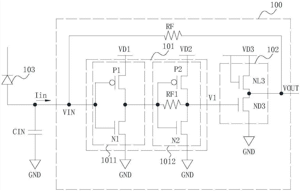
[0030] The inverting amplifying unit 102 includes a third N-type transistor NL3 and a fourth N-type transistor ND3, the first terminal and the second terminal of the third N-type transistor NL3 are used to receive the third DC voltage VD3, and the third terminal is used to output amplifying the voltage signal VOUT; the first end of the fourth N-type transistor ND3 is coupled to the third end of the third N-type transistor NL3, and the second end is coupled to the output end of the equivalent secondary amplification module 101 for receiving the first voltage Signal V1, the third terminal is grounded.

[0031] The equivalent secondary amplifying module 101 of the transimpedance amplifier 100, the inverting amplifying unit 102 and the feedback resistor RF form a three-stage operational amplifier, and the inverting amplifying unit is used as one of the first-stage amplifying units in the three-stage operational amplifier, using two N-type The structure of the transistor is used to...

Embodiment 2

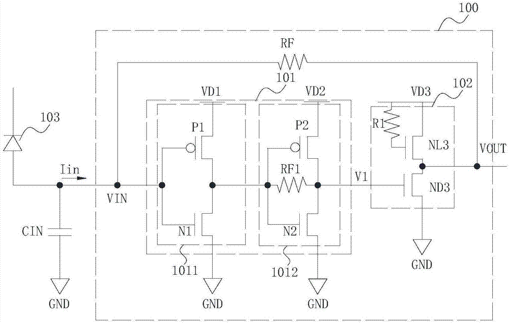
[0034] Such as figure 2 As shown, as another embodiment of the present invention, the inverting amplifying unit 102 further includes a resistor R1, one end of the resistor R1 receives the third DC voltage, and the other end is coupled to the second end of the third N-type transistor N3. The two terminals are coupled with a resistor, so that the resistor R1 acts as an active inductor, which can increase the bandwidth of the inverting amplifier unit 102 , thereby increasing the gain-bandwidth product of the entire transimpedance amplifier 100 .

[0035] In order to reduce the voltage drop across the third N-type transistor NL3, in the embodiment of the present invention, the third N-type transistor NL3 adopts Native NFET.

[0036] In another embodiment of the present invention, the positions of the equivalent secondary amplifying module 101 and the inverting amplifying unit 102 are exchanged, and the input end of the inverting amplifying unit 102 is coupled to the photodiode 10...

Embodiment 3

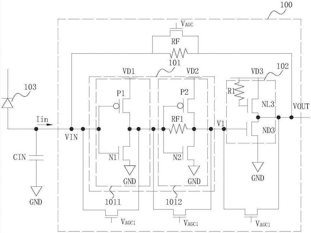
[0038] Such as image 3 As shown, as another embodiment of the present invention, each of the three units for signal amplification may be provided with an N-type transistor between its own input terminal and output terminal, and an N-type transistor is also provided at both ends of the feedback resistor. This N-type transistor enables AGC control (Automatic Gain Control) of the transimpedance amplifier.

[0039] In addition to the above-mentioned functions, if noise and sensitivity are not the main design goals of the transimpedance amplifier 100, the conductance of the P-type transistor and the N-type transistor in the transimpedance amplifier 100 can be reduced. If the conductance is reduced, the current consumption will be reduced, thereby realizing transimpedance amplifier 100. The power consumption of the impedance amplifier 100 is reduced.


PUM


Abstract

The invention provides a trans-impedance amplifier. The amplifier comprises an equivalent secondary amplification module, an anti-phase amplification unit and a feedback resistor; the input end of the equivalent secondary amplification module is coupled to a photodiode and used for inputting a voltage signal, and the output end of the equivalent secondary amplification module outputs a first voltage signal subjected to secondary amplification; the anti-phase amplification unit is coupled to the output end of the equivalent secondary amplification module and used for connecting the first voltage signal and outputting an amplified voltage signal subjected to anti-phase amplification, the anti-phase amplification unit comprises a third N-shaped transistor and a fourth N-shaped transistor coupled with the third N-shaped transistor, the third N-shaped transistor is used for receiving a third direct voltage signal, the fourth N-shaped transistor is used for receiving the first voltage signal output through the equivalent secondary amplification module, and the common connection end of the third N-shaped transistor and the fourth N-shaped transistor outputs an amplified voltage signal; the feedback resistor is couple with the input end of the equivalent secondary amplification module and the output end of the anti-phase amplification unit. The trans-impedance amplifier can not be constrained by original conditions, and can increase the resistance, reduce the input noise, and improve the sensitivity.

Description

technical field [0001] The invention relates to the technical field of CMOS, in particular to a transimpedance amplifier with enlarged gain, reduced noise and simple design. Background technique [0002] The full name of transimpedance amplifier (TIA) is trans-impedance amplifier, which is a type of amplifier. The type of amplifier is defined according to the type of its input and output signals. Due to the advantages of high bandwidth, TIA is generally used in high-speed circuits, such as optical transmission and communication systems. [0003] The equivalent input noise of a transimpedance amplifier is one of the important indicators to measure its transmission performance. In order to improve the sensitivity of the transimpedance amplifier, it is necessary to reduce the noise output, and one of the ways to reduce the noise output can be by increasing the transimpedance. In theory, the larger the transimpedance, the smaller the noise, but the transconductance is limited b...

Claims


Application Information

Patent Timeline
Patent Type & Authority Applications(China)
IPC IPC(8): H03F1/26H03F3/08H03F3/45H03F3/68
CPCH03F1/26H03F3/082H03F3/45179H03F3/68H03G1/0029H03F3/3022H03G3/3084H03F3/45475
Inventor 邹何洪
Owner HANGZHOU HONGXIN MICROELECTRONICS TECH CO LTD
Why Eureka
Try Eureka