Eureka AIR delivers breakthrough ideas for toughest innovation challenges, trusted by R&D personnel around the world.

A high-speed and high-gain avalanche photodetector and its preparation method

An avalanche photoelectric and detector technology, applied in the field of detectors, can solve the problems of tunnel breakdown, increased device tunneling current, large APD gain-bandwidth product, etc., to achieve low excess noise, reduce junction capacitance, and reduce dark Effects of current and carrier stacking

Active Publication Date: 2022-05-03
INST OF SEMICONDUCTORS - CHINESE ACAD OF SCI
View PDF4 Cites 0 Cited by
  • Summary
  • Abstract
  • Description
  • Claims
  • Application Information

AI Technical Summary

Problems solved by technology

[0004] In addition, the main factor limiting the APD bandwidth at high gain is the avalanche gain time of the multiplication region, the thinner the multiplication region, the larger the gain-bandwidth product of the APD
However, the thin multiplication region requires a higher electric field strength to cause avalanche multiplication, which will increase the tunneling current of the device, and tunnel breakdown will occur in severe cases

Method used


Image

  • A high-speed and high-gain avalanche photodetector and its preparation method
  • A high-speed and high-gain avalanche photodetector and its preparation method
  • A high-speed and high-gain avalanche photodetector and its preparation method

Examples


Embodiment Construction

[0047] Hereinafter, embodiments of the present disclosure will be described with reference to the drawings. It should be understood, however, that these descriptions are exemplary only, and are not intended to limit the scope of the present disclosure. In the following detailed description, for purposes of explanation, numerous specific details are set forth in order to provide a thorough understanding of the embodiments of the present disclosure. It may be evident, however, that one or more embodiments may be practiced without these specific details. Also, in the following description, descriptions of well-known structures and techniques are omitted to avoid unnecessarily obscuring the concept of the present disclosure.

[0048] The terminology used herein is for the purpose of describing particular embodiments only, and is not intended to be limiting of the present disclosure. The terms "comprising", "comprising", etc. used herein indicate the presence of stated features, ...


PUM

PropertyMeasurementUnit
thicknessaaaaaaaaaa
thicknessaaaaaaaaaa
thicknessaaaaaaaaaa

Abstract

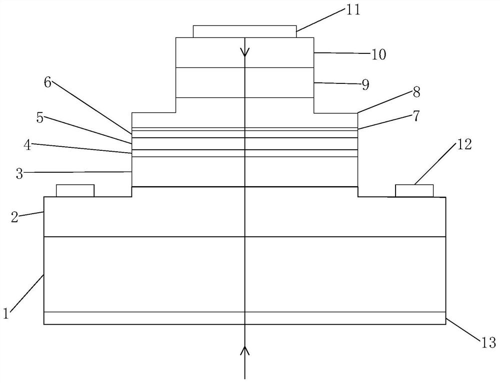
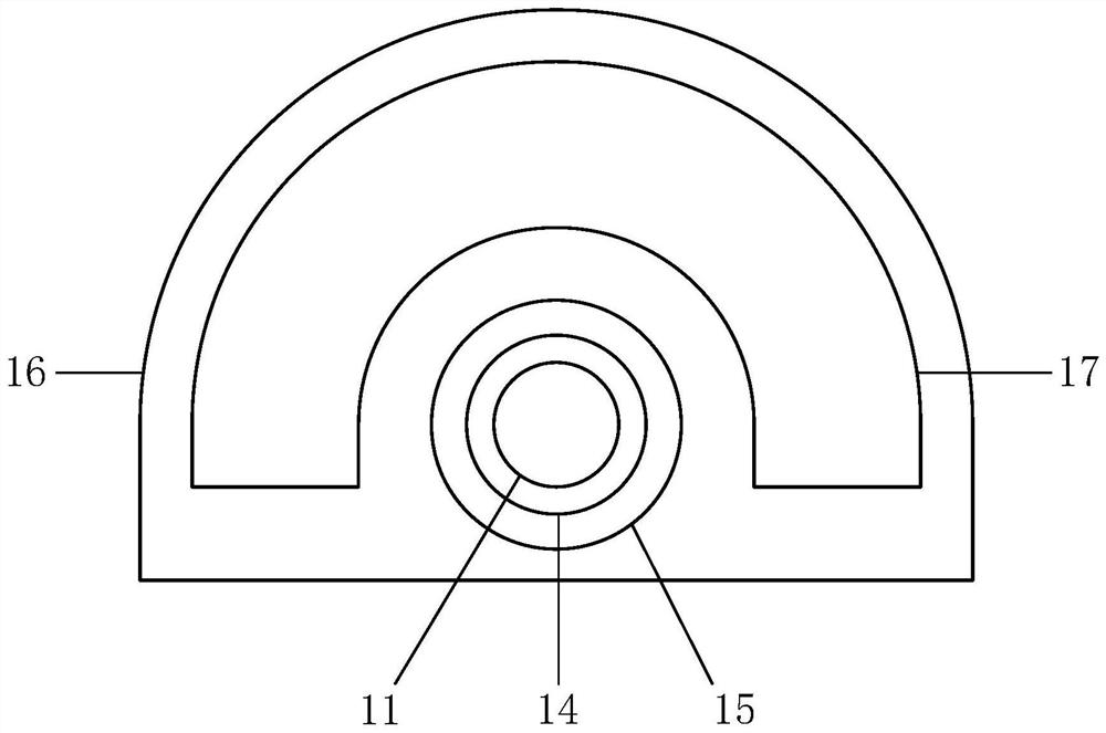
The present disclosure provides a high-speed and high-gain avalanche photodetector and its preparation method, the chip of which includes three steps arranged from top to bottom; wherein: the first step includes P electrodes arranged in sequence from top to bottom, The first ohmic contact layer, the first absorption layer, and the upper part of the second absorption layer; the second step, including the lower part of the second absorption layer, the transition layer, the first charge layer, the multiplication layer, and the second charge layer arranged in sequence from top to bottom layer, the transition layer and the upper part of the second ohmic contact layer; the third step, including the lower part of the second ohmic contact layer and the insulating substrate arranged in sequence from top to bottom; the horizontal projected area of ​​the three steps increases in turn. The chip multiplication layer is made of ultra-thin InAlAs material. The three-level step chip is upside-down bonded on the substrate.

Description

technical field [0001] The disclosure relates to the technical field of detectors, in particular to a high-speed and high-gain avalanche photodetector. Background technique [0002] With people's increasing demand for information transmission, there are higher requirements for the transmission speed and transmission distance of optical communication. As an important receiving device in optical communication, semiconductor photodetector plays a pivotal role. Compared with PIN detectors, avalanche photodetectors have improved responsivity to optical signal detection due to their internal gain to photocurrent. Therefore, high-speed and high-gain APDs are increasingly used in optical communications. The main indicators for evaluating APD performance include 3dB bandwidth, dark current, responsivity, and gain-bandwidth product. [0003] Commonly used high-speed APDs use a SAGCM structure that separates and absorbs charge multiplication. In order to improve the response speed ...

Claims


Application Information

Patent Timeline
Patent Type & Authority Patents(China)
IPC IPC(8): H01L31/0352H01L31/0224H01L31/0304H01L31/107H01L31/18
CPCH01L31/107H01L31/1075H01L31/1852H01L31/1844H01L31/03529H01L31/035281H01L31/022408H01L31/03046Y02P70/50
Inventor 杨晓红王睿王晖何婷婷
Owner INST OF SEMICONDUCTORS - CHINESE ACAD OF SCI
Why Eureka
Eureka Blog
Learn More