

Process for producing group III nitride compound semiconductor light emitting device, group III nitride compound semiconductor light emitting device and lamp
a technology of compound semiconductors and light emitting devices, which is applied in the direction of semiconductor devices, lasers, semiconductor lasers, etc., can solve the problems of poor crystallinity of buffer layers, inability to produce excellent crystallinity even if the method is stably used, and inability to provide excellent crystallinity
- Summary
- Abstract
- Description
- Claims
- Application Information
AI Technical Summary
Benefits of technology
Problems solved by technology
Method used
Image

Examples
example 1
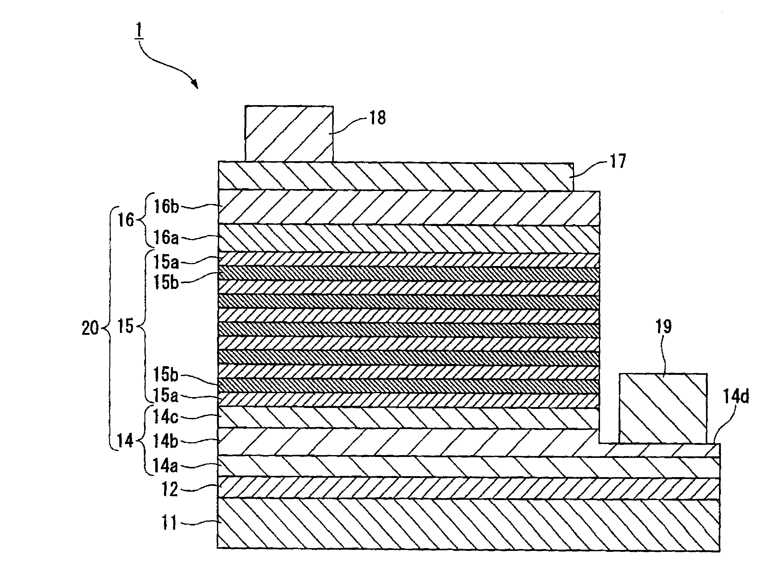
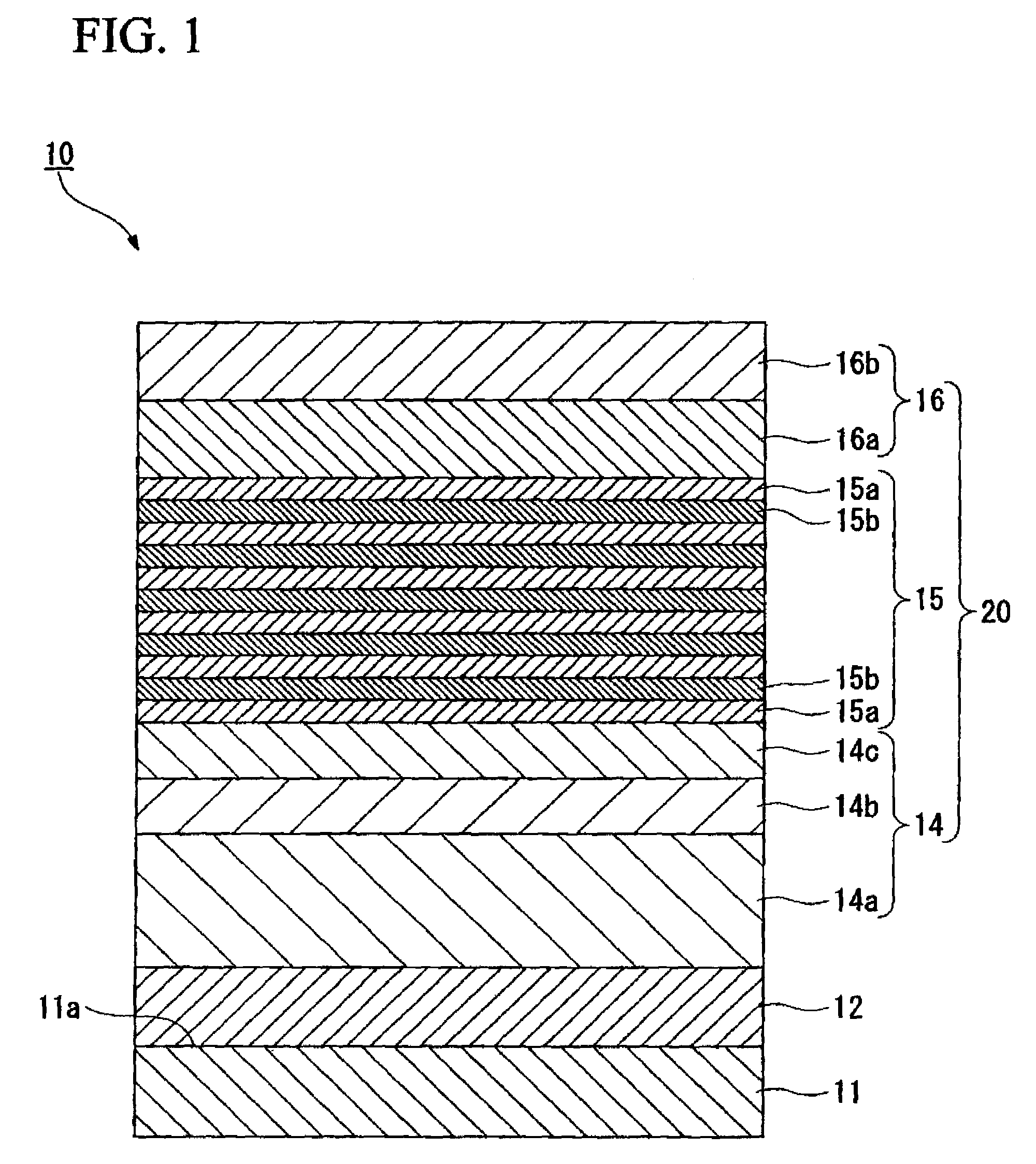
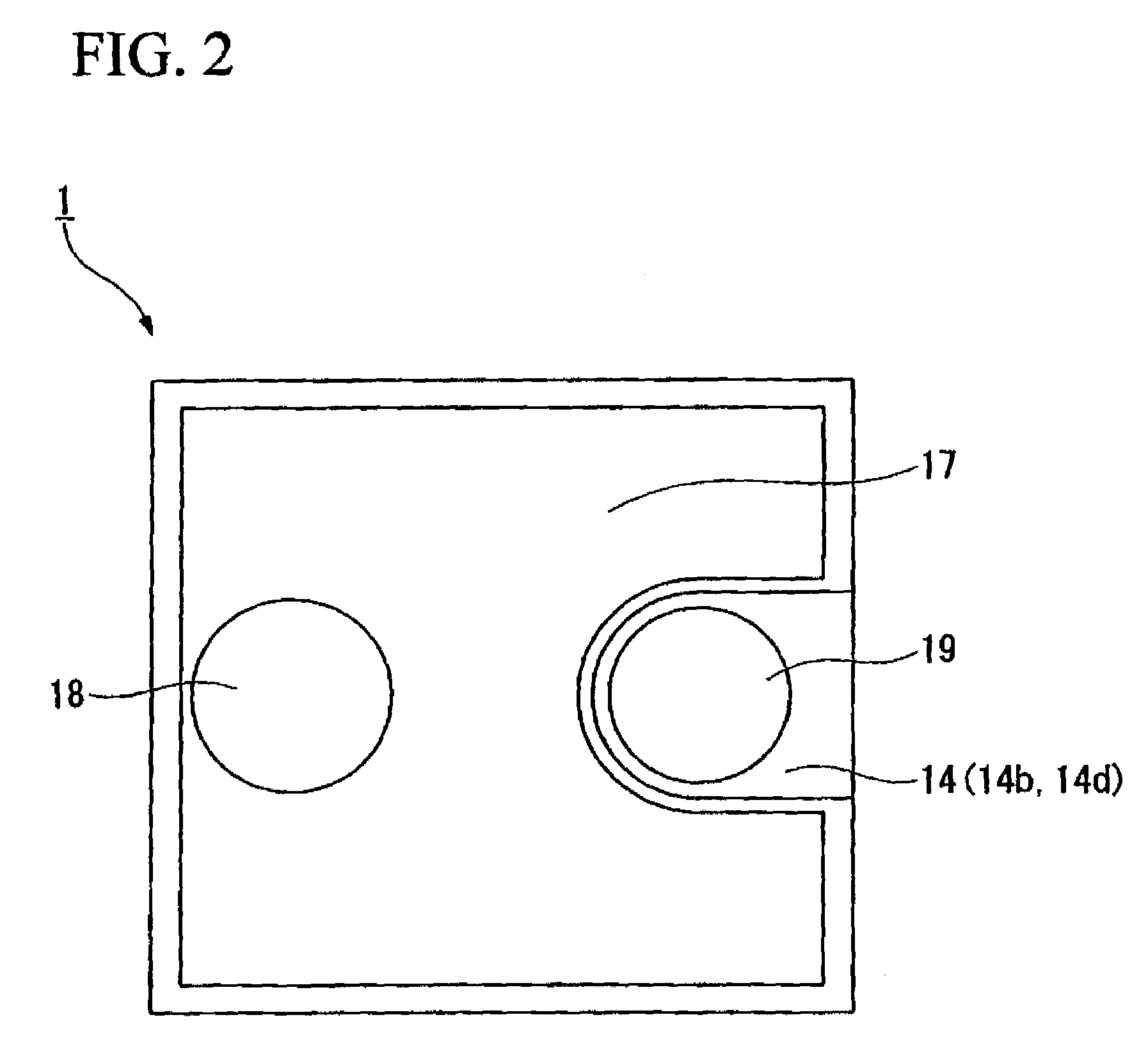
[0143]FIG. 1 is a schematic view showing a sectional structure of a laminated semiconductor of a group III nitride compound semiconductor light emitting device produced in this Example.
[0144]In this example, an aggregate of a columnar crystal consisting of AlN was formed on a c surface of the substrate 11 consisting of sapphire, as the buffer layer 12 using an RF sputtering method. Each of the ground layer 14a and the n-type contact layer 14b was formed as the n-type semiconductor layer 14 thereon using an RF sputtering method, and the n-type clad layer 14c was formed onto the n-type contact layer 14b using a MOCVD method. Also, the light emitting layer 15 was formed thereon using a MOCVD method, and then each of the p-type clad layer 16a and the p-type contact layer 16b was laminated in this order as the p-type semiconductor layer 16 onto the light emitting layer 15 using a sputtering method.
[0145]At first, the substrate 11 consisting of sapphire only one surface of which has been ...
PUM
 Abstract
Description
Claims
Application Information