Method for growing nitride light-emitting diode (LED) epitaxial wafer with reversed V-shaped coarsening surface

A technology for LED epitaxial wafers and surface roughening, which is applied to electrical components, circuits, semiconductor devices, etc.

Inactive Publication Date: 2013-03-13
YANGZHOU ZHONGKE SEMICON LIGHTING
View PDF3 Cites 4 Cited by
  • Summary
  • Abstract
  • Description
  • Claims
  • Application Information

AI Technical Summary

Problems solved by technology

The refractive index of GaN is 2.4, and the refractive index of air is 1. A large part of the light generated by electron-hole recombination cannot be extracted due to t

Method used


Image

  • Method for growing nitride light-emitting diode (LED) epitaxial wafer with reversed V-shaped coarsening surface
  • Method for growing nitride light-emitting diode (LED) epitaxial wafer with reversed V-shaped coarsening surface
  • Method for growing nitride light-emitting diode (LED) epitaxial wafer with reversed V-shaped coarsening surface

Examples


Embodiment 1

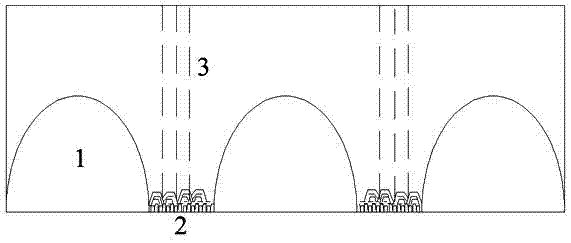
[0028] 1. Growing an AlN buffer layer 2 on a sapphire pattern substrate 1: the growth temperature is 1000° C., the pressure is 500 mbar, and the thickness of the grown AlN buffer layer 2 is 30 nm. Then the temperature was raised to 1030°C for nucleation and recrystallization. The GaN epitaxial film was grown under the conditions of a pressure of 650 mbar and a N:Ga molar ratio of 942:1, and the island-like GaN closed rapidly to form a continuous u-GaN epitaxial film. Dislocations 3 will form at the closure of two island-shaped GaN with a dislocation density of 1×10 8 cm -2 ~1×10 9 cm -2 ,Such as figure 1 shown.

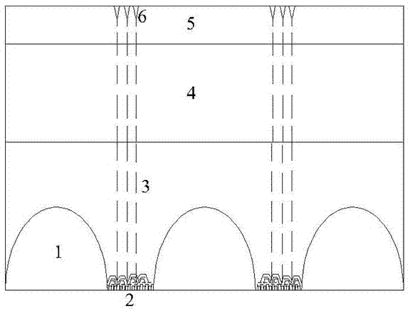
[0029] 2. According to the conventional method, on the u-GaN epitaxial film, the n-GaN layer 4 and the multi-quantum well MQWs 5 needed for the LED are epitaxially grown sequentially. The dislocations are released to a certain extent at the multiple quantum well MQWs5, forming a "V"-shaped pit 6, such as figure 2 shown.

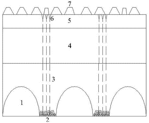
[0030] 3. Epitaxial growth of pGaN o...

Embodiment 2

[0034] 1. Al growth on the sapphire pattern substrate 1 2 GaN buffer layer 2: the growth temperature is 1200° C., the pressure is 600 mbar, and the thickness of the grown AlN buffer layer 2 is 30 nm. Then the temperature was raised to 1300°C for nucleation and recrystallization. The GaN epitaxial film was grown under the conditions of a pressure of 650 mbar and a N:Ga molar ratio of 942:1, and the island-like GaN closed rapidly to form a continuous u-GaN epitaxial film. Dislocations 3 will form at the closure of two island-shaped GaN with a dislocation density of 1×10 8 cm -2 ~1×10 9 cm -2 .

[0035] 2. According to a conventional method, sequentially epitaxially grow the nGaN layer 4 and the multi-quantum well MQWs 5 required for the GaN-based LED on the u-GaN.

[0036] 3. Epitaxial growth of pGaN at low temperature and then high temperature on the multi-quantum well MQWs5: Mg element is used for P-type doping, and the doping concentration is 1×10 17 ~5×10 19 cm...


PUM

PropertyMeasurementUnit
Dislocation densityaaaaaaaaaa
Thicknessaaaaaaaaaa
Thicknessaaaaaaaaaa

Abstract

A method for growing a nitride light-emitting diode (LED) epitaxial wafer with a reversed V-shaped coarsening surface belongs to the photoelectric technology field of semiconductors. Firstly a high dislocation density gallium nitride (GaN) epitaxial film is achieved on a sapphire substrate, and the method for growing a nitride LED with the reversed V-shaped coarsening surface is achieved through density. Dislocation can be released on a multi-quantum wells (MQWs) surface to form a V-shaped pit, low-temperature high-pressure growth is used for growing pGaN, an expansion free-path of the Ga element at low temperature and high pressure is short, three-dimensional growth serves as a main mode, and the V-shaped pit is not easy to fill in a growing process. Therefore, the V-shaped pit is equivalently released in the growing process, further a pGaN coarsening surface with the reversed V-shaped surface is formed, accordingly the nitride LED with the reversed V-shaped coarsening surface is obtained, and light intensity is 100% promoted.

Description

technical field [0001] The invention belongs to the technical field of semiconductor optoelectronics, in particular to the technical field of processing a nitride LED epitaxial wafer with a roughened surface. Background technique [0002] Gallium Nitride (GaN)-based LED, as a solid-state light source, has been hailed as the second revolution in the history of human lighting after Edison invented the electric light for its advantages of high efficiency, long life, and environmental protection. It has become an international semiconductor and lighting field. The focus of R&D and industry attention. However, GaN-based LEDs are currently entering the field of general lighting, and they still face many difficulties in terms of technology and cost. [0003] At present, one of the main problems faced by GaN-based LED brightness improvement is the problem of light efficiency extraction. The refractive index of GaN is 2.4, and the refractive index of air is 1. A large part of the l...

Claims


Application Information

Patent Timeline
IPC IPC(8): H01L33/22
Inventor 李鸿渐李盼盼李志聪李璟王国宏
Owner YANGZHOU ZHONGKE SEMICON LIGHTING
Why Eureka
Try Eureka