Polishing method, polishing apparatus and GaN wafer

a polishing apparatus and polishing technology, applied in the direction of grinding machine components, manufacturing tools, lapping machines, etc., can solve the problems of difficult processing of cmp, inability to fully remove denatured layers by cmp, and in general suited photoelectrochemical etching methods for processing and flattening of substrate surfaces, etc., to achieve sufficient surface accuracy and short processing time

Active Publication Date: 2016-01-12
OSAKA UNIV +1
View PDF13 Cites 4 Cited by
  • Summary
  • Abstract
  • Description
  • Claims
  • Application Information

AI Technical Summary

Benefits of technology

[0009]Thus, when processing and flattening a surface of a Ga element-containing compound semiconductor substrate, such as a GaN substrate, having surface irregularities by a conventional polishing method, dissolution of Ga oxide will occur in recessed portions of the surface of the substrate as well as in raised portions. This makes it difficult to selectively remove the tops of the raised portions of the substrate surface having surface irregularities while inhibiting removal in the recessed portions of the substrate surface, and necessitates a considerably long time to flatten the substrate surface.
[0037]According to the present invention, a surface of a substrate of a Ga element-containing compound semiconductor, such as GaN, GaAs or GaP, can be polished and flattened in a significantly shortened processing time while ensuring sufficient surface accuracy.

Problems solved by technology

The photoelectrochemical etching method, however, is not generally suited for processing and flattening of a surface of a substrate because this method lacks a flattening reference and, in addition, involves defect selectivity, and the like.
Because CMP involves a mechanical action, such a denatured layer cannot be fully removed by CMP.
Further, it is generally difficult for CMP to process and flatten a surface of a Ga element-containing compound semiconductor substrate at a sufficient processing rate.
It is, however, generally difficult for this method to process and flatten a surface of a Ga element-containing compound semiconductor substrate at a sufficient processing rate.

Method used


Image

  • Polishing method, polishing apparatus and GaN wafer
  • Polishing method, polishing apparatus and GaN wafer
  • Polishing method, polishing apparatus and GaN wafer

Examples


experiment 1

[Demonstration Experiment 1]

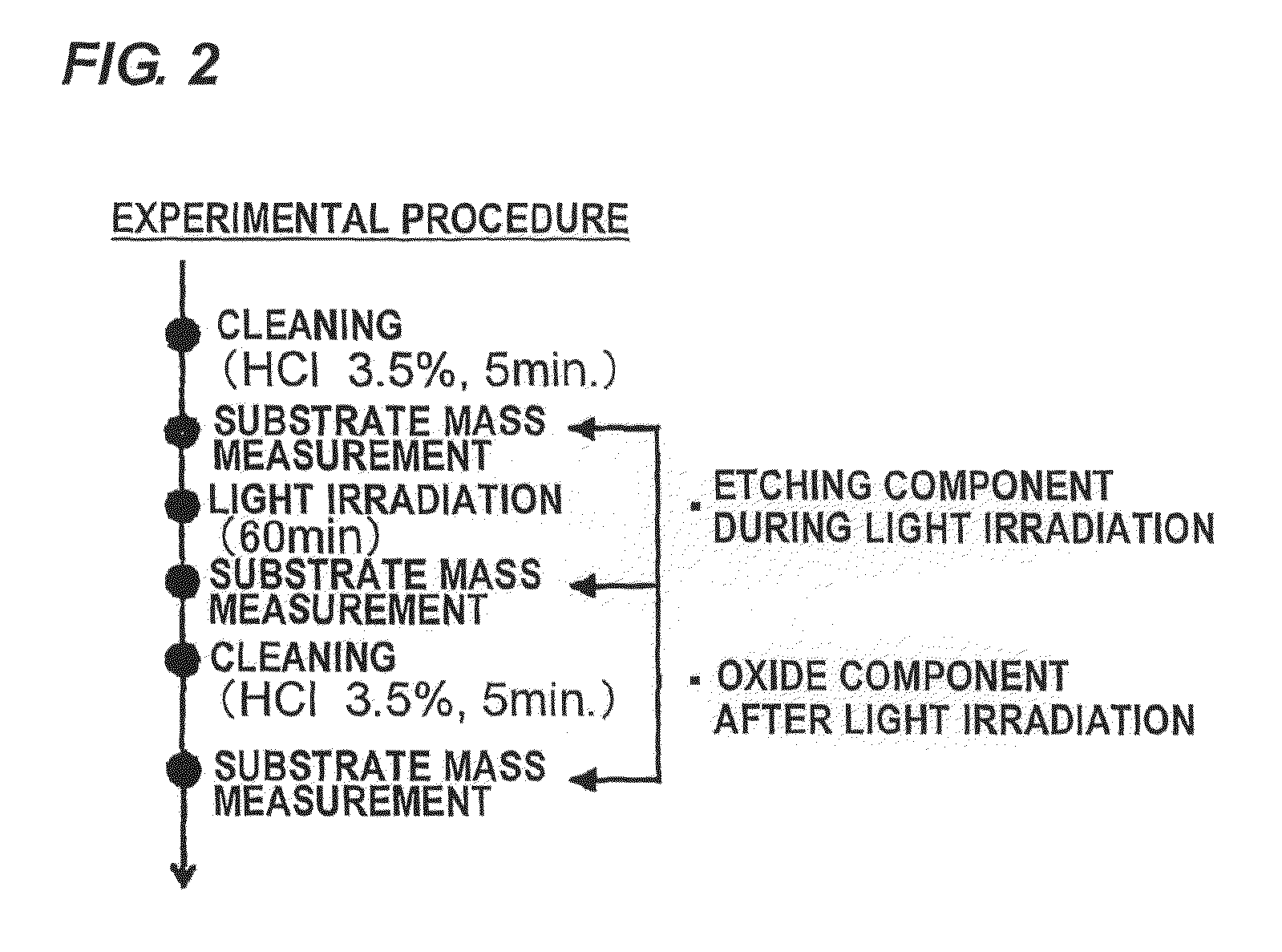
[0080]FIG. 2 shows the procedure of the experiment. As shown in FIG. 2, a GaN substrate was cleaned with an aqueous solution of 3.5% HCl for 5 minutes. The mass (mass 1) of the GaN substrate was then measured. Thereafter, the GaN substrate was placed in a phosphate buffer solution, and a surface of the GaN substrate was irradiated with light for 60 minutes to produce a Ga oxide on the surface. The mass (mass 2) of the GaN substrate was then measured. Further, “etching component during light irradiation” was determined from the mass difference (mass 2−mass 1). Next, the GaN substrate was cleaned with an aqueous solution of 3.5% HCl for 5 minutes, followed by measurement of the mass (mass 3) of the GaN substrate. “Oxide component after light irradiation” was determined from the mass difference (mass 3−mass 2).

[0081]The“etching component during light irradiation” indicates the mass of Ga oxide that dissolved in the phosphate buffer solution during the light ...

experiment 2

[Demonstration Experiment 2]

[0084]A GaN substrate was placed in a phosphate buffer solution containing 10 ppm of Ga ions and having a pH of 6.86, and a surface of the GaN substrate was irradiated with light for 3 hours. The GaN substrate surface was observed using an optical microscope before and after the light irradiation. FIG. 4 shows an optical microscopic image of the GaN substrate surface before the light irradiation, and FIG. 5 shows an optical microscopic image of the GaN substrate surface after the light irradiation. As can be seen from FIGS. 4 and 5, there is no significant change in the surface state of the GaN substrate, with no worsening of the surface roughness, before and after the light irradiation.

[0085]A comparative experiment was conducted in which a GaN substrate was placed in a phosphate buffer solution containing no Ga ions and having a pH of 6.86, and a surface of the GaN substrate was irradiated with light for 3 hours. The GaN substrate surface was observed u...

example 1

[0140]Using the polishing apparatus shown in FIG. 8 and using, as a processing solution, a phosphate buffer solution having a pH of 6.86 and containing 10 ppm of Ga ions, polishing of a surface of a Ga substrate was carried out with a polishing tool, composed of quartz glass which is an acidic solid catalyst, for 3 hours while irradiating the surface with ultraviolet light, having a peak emission wavelength of 365 nm, emitted from a light source. FIGS. 17 and 18 show optical microscopic images of the surface of the GaN substrate after processing.


PUM

PropertyMeasurementUnit
flatnessaaaaaaaaaa
PV surface flatnessaaaaaaaaaa

Abstract

A polishing method can process and flatten, in a practical processing time and with high surface accuracy, a surface of a substrate of a Ga element-containing compound semiconductor. The polishing method includes: bringing a Ga element-containing compound semiconductor substrate (16) into contact with a polishing tool (10) in the presence of a processing solution (14) comprising a neutral pH buffer solution containing Ga ions; irradiating a surface of the substrate with light or applying a bias potential to the substrate, or applying a bias potential to the substrate while irradiating the surface of the substrate with light, thereby forming Ga oxide (16a) on the surface of the substrate; and simultaneously moving the substrate and the polishing tool relative to each other to polish and remove the Ga oxide formed on the surface of the substrate.

Description

TECHNICAL FIELD[0001]The present invention relates to a polishing method and a polishing apparatus, and more particularly to a polishing method and a polishing apparatus for processing and flattening a surface (surface to be processed) of a substrate, such as an elemental substrate of a compound semiconductor containing Ga (gallium) element or a bonded substrate (epitaxial substrate) having a layer of Ga element-containing compound semiconductor.[0002]The present invention also relate to a GaN wafer produced by the polishing method.BACKGROUND ART[0003]As a chemical processing method which takes the place of mechanical processing and is capable of processing a surface of a substrate without producing a lattice defect, a so-called photoelectrochemical etching method is known, which performs etching of a surface of a substrate in an acidic or basic processing solution by irradiating the surface of the substrate with ultraviolet rays or by applying a potential bias to the substrate. The...

Claims


Application Information

Patent Timeline
Patent Type & Authority Patents(United States)
IPC IPC(8): H01L21/461B24B37/005H01L21/304
CPCB24B37/0056
Inventor SANO, YASUHISAYAMAUCHI, KAZUTOMURATA, JUNJISADAKUNI, SHUNYAGI, KEITA
Owner OSAKA UNIV
Why Eureka
Try Eureka