Low skew clock distribution tree
a clock distribution and low skew technology, applied in the field of integrated circuit memory, can solve the problems of loss of clock and data performance, unmatched widths and spacings of various clock busses and clock bus segments, and increasing clock and signal skew, so as to maximize valid times and minimize clock skew.
- Summary
- Abstract
- Description
- Claims
- Application Information
AI Technical Summary
Benefits of technology
Problems solved by technology
Method used
Image
Examples
first embodiment
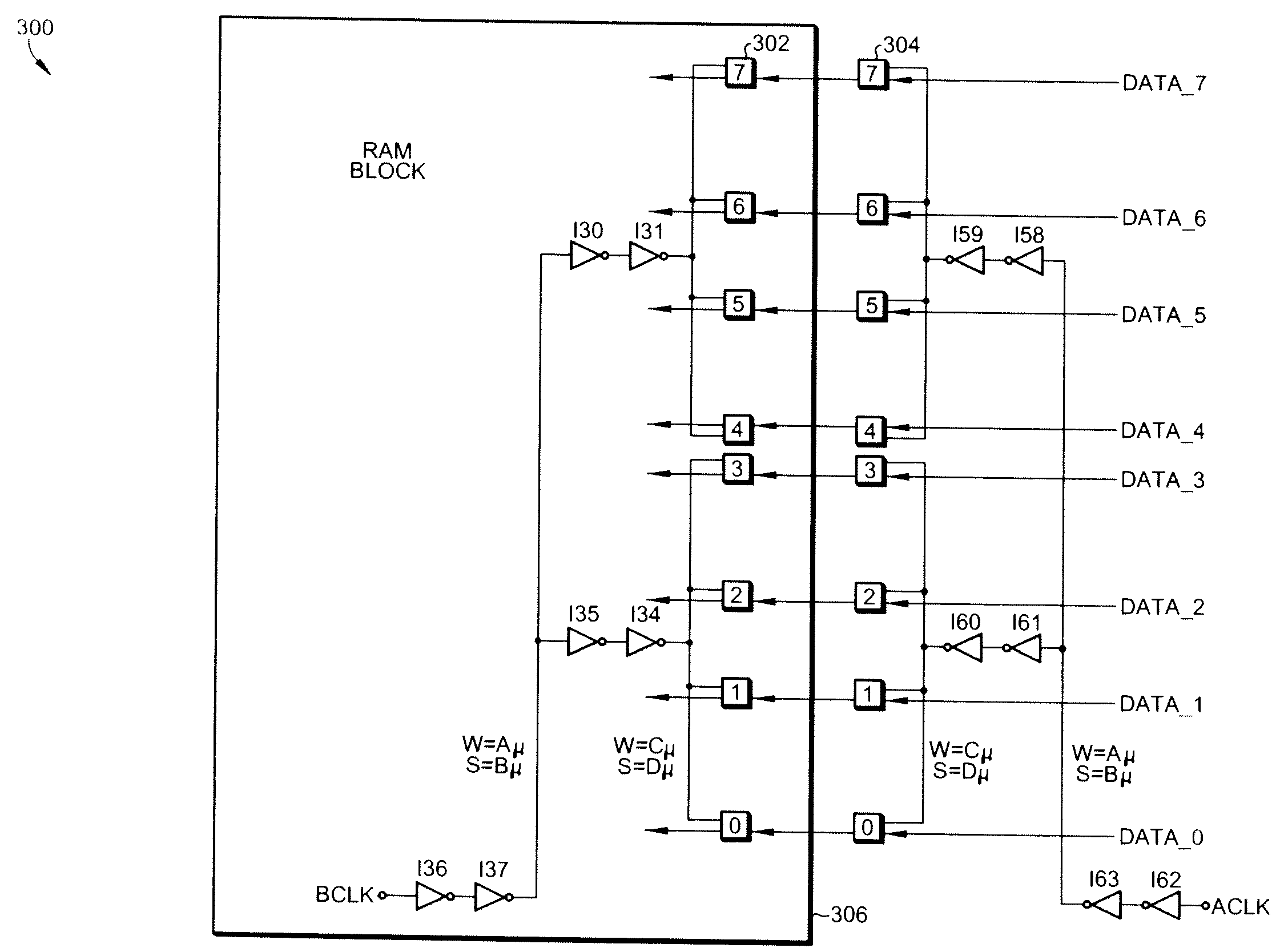
[0018]A clock distribution tree circuit is shown for a portion of an integrated circuit memory 300 in FIG. 3 according to the present invention. Integrated circuit memory 300 includes input buffers 302 designated 0 through 7 resident in RAM block 306. Each input buffer has a data input, a data output, and a clock input. Integrated circuit memory 300 also includes data drivers 204 designated 0 through 7, corresponding to each of the input buffers. The clock input, data input, and the data output of the data drivers 304 are all shown in FIG. 3. The data drivers 304 are clocked by a first clock distribution tree including inverters I59-I63. Inverters I58 and I59 clock data drivers 4 through 7 and inverters I60 and I61 clock data drivers 0 through 3. In turn, inverters I62 and I63 drive inverters I58 and I61. The input buffers 302 are clocked by a second clock distribution tree mirroring the first clock distribution tree according to an aspect of the present invention including inverter...
second embodiment
[0020]A clock distribution tree circuit is shown for a portion of an integrated circuit memory 400 in FIG. 4 according to the present invention. Integrated circuit memory 400 includes input buffers 402 designated 0 through 7 resident in RAM block 406. Each input buffer has a data input, a data output, and a clock input. Integrated circuit memory 400 also includes data drivers 404 designated 0 through 7, corresponding to each of the input buffers. The clock input, data input, and the data output of the data drivers 404 are all shown in FIG. 4. The data drivers 404 are clocked by a first clock distribution tree including inverters I58-I59 and I62-I63. The input buffers 402 are clocked by a second clock distribution tree mirroring the first clock distribution tree according to an aspect of the present invention including inverters I30-I31 and I36-I37. Inverter I62 receives the ACLK clock signal, and inverter I36 receives the BCLK signal. The width W (Aμ) and spacings S (Bμ) of the firs...
PUM
 Abstract
Description
Claims
Application Information


