Light emitting diode package

a technology of light-emitting diodes and light-emitting diodes, which is applied in the direction of basic electric elements, electrical apparatus, and semiconductor devices, can solve the problems of limited primary elements of materials, difficult to form a reflecting face, and inadequacies of led packages for high-luminance emitting-light, etc., to achieve convenient application of high-luminance leds, easy control of luminance, and efficient emitted

Active Publication Date: 2009-09-22
SUZHOU LEKIN SEMICON CO LTD
View PDF6 Cites 82 Cited by
  • Summary
  • Abstract
  • Description
  • Claims
  • Application Information

AI Technical Summary

Benefits of technology

[0021]For the LED package of the embodiment of the invention, it is easy to control luminance according to the luminance and an angle. Since heat is efficiently emitted, the LED package is easily applicable to a high luminance LED. Also, by manufacturing the LED package with a simple construction, the manufacturing process is convenient and the cost is low.

Problems solved by technology

Especially, in order to obtain distribution of a luminance angle according to high luminance and user requirements, the primary element of the materials is limited.
However, since the construction of the LED package using the molding resin does not have high enough thermal resistance for heat generated by high luminance light, the LED package is not appropriate for the high-luminance emitting-light.
Therefore, it is difficult to form a reflecting face which can control the luminance angle by making a predetermined inclined plane inside of the cavity.
In addition, it makes a manufacturing process complicated and increases the cost that the ceramic substrate 22 supplying the cavity is made of the plurality of substrates which are laminated.
Also, since the heat which is generated by the high luminance light is emitted through only the electrode 23, emitting heat is not rapid, which has a bad influence on characteristics of operation of the LED device 25.
In addition, it takes manufacturing time longer and increase the cost, because the ceramic substrate 22 is made of the plurality of substrates which are laminated.

Method used


Image

  • Light emitting diode package
  • Light emitting diode package
  • Light emitting diode package

Examples


Embodiment Construction

[0027]Hereinafter, preferred embodiments of the present invention will be described in detail with reference to the accompanying drawings.

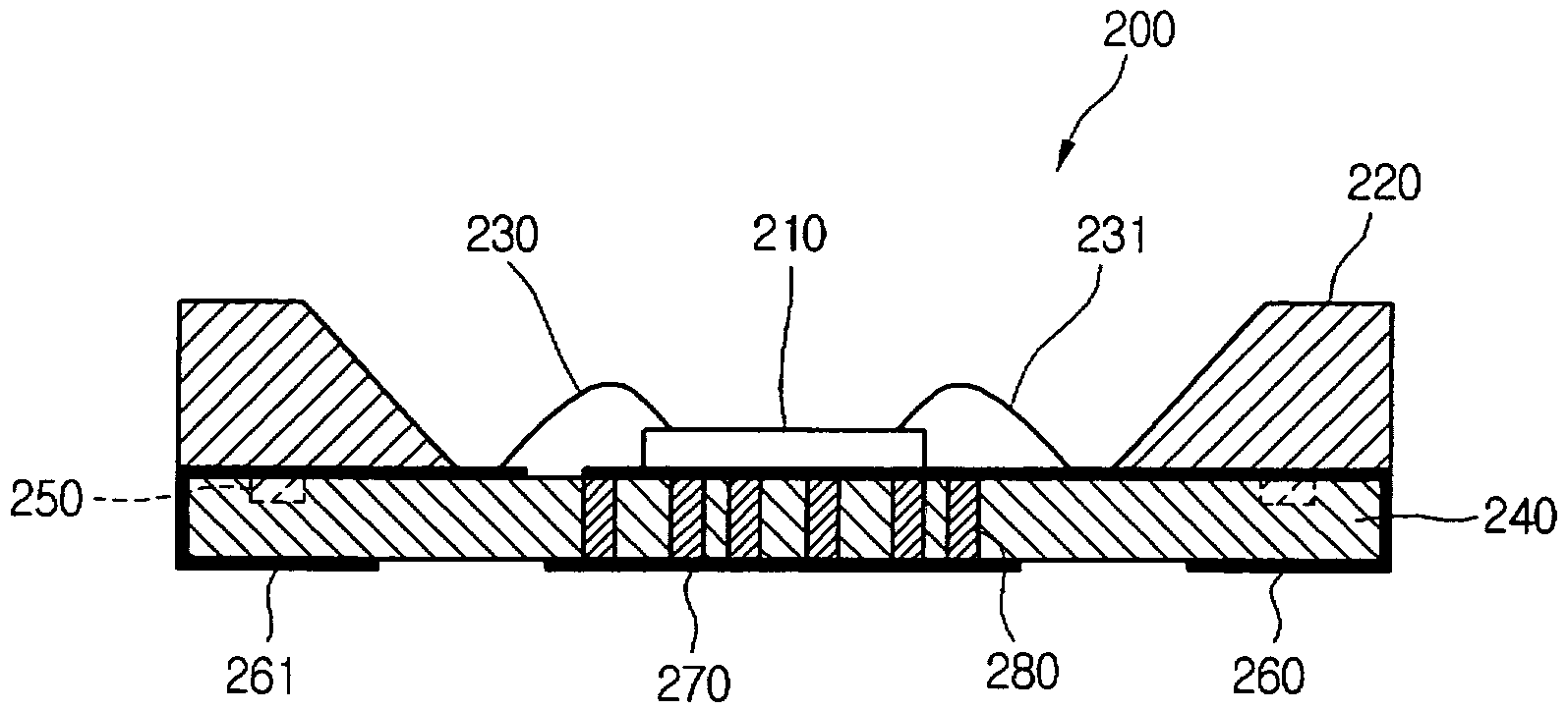
[0028]FIG. 2 is a sectional view illustrating an LED package 200 according to the present invention.

[0029]Referring to FIG. 2, the LED package 200 of the present invention includes a ceramic substrate 240, an LED 210 mounted on the upper side of the ceramic substrate 240, a reflecting member 220 formed around the portion in which the LED 200 is mounted, an electrode 260 and 261 and wire 230 and 231 provided on the upper side of the ceramic substrate 240 and electrically connected to the LED 210, and a heat sink 270 and a heatsink hole 280 emitting out heat generated from the LED 210.

[0030]In detail, since the ceramic substrate 240 is provided as a single layer, it is possible to reduce the manufacturing process and take the manufacturing time shorter.

[0031]Also, it is advantageous for the improvement of luminance and the control of a luminance ang...


PUM


Abstract

Provided is an LED package. It is easy to control luminance according to the luminance and an angle applicable. Since heat is efficiently emitted, the LED package is easily applicable to a high luminance LED. The manufacturing process is convenient and the cost is reduced. The LED package includes a substrate, an electrode, an LED, and a heatsink hole. The electrode is formed on the substrate. The LED is mounted in a side of the substrate and is electrically connected to the electrode. The heatsink hole is formed to pass through the substrate, for emitting out heat generated from the LED.

Description

BACKGROUND OF THE INVENTION[0001]1. Field of the Invention[0002]The present invention relates to a light emitting diode and a package of a light emitting diode.[0003]2. Description of the Related Art[0004]A light emitting diode (LED) is a light emitting device constituting a light source by using compound semiconductor materials such as GaAs, AlGaAs, GaN, InGaN, and AlGaInP. The LED has the advantage of emitting various colors on materials of the semiconductor.[0005]Generally, the characteristics of the LED are determined according to high-luminance light-emitting, luminance, color range of the emitted light, and the like. The characteristics of the LED device are primary determined by the compound semiconductor materials used in the LED device. Also, the characteristics are secondly determined by package construction for mounting a chip. Especially, in order to obtain distribution of a luminance angle according to high luminance and user requirements, the primary element of the mat...

Claims


Application Information

Patent Timeline
Patent Type & Authority Patents(United States)
IPC IPC(8): H01L33/00H01L33/48H01L33/60H01L33/64
CPCH01L33/60H01L33/642H01L33/62H01L33/58H01L33/486H01L33/647H01L2224/48091H01L2224/48247H01L2224/48227H01L2924/00014H01L33/483H01L33/52H01L33/64
Inventor KIM, WAN HO
Owner SUZHOU LEKIN SEMICON CO LTD
Why Eureka
Try Eureka