Post etch wafer surface cleaning with liquid meniscus

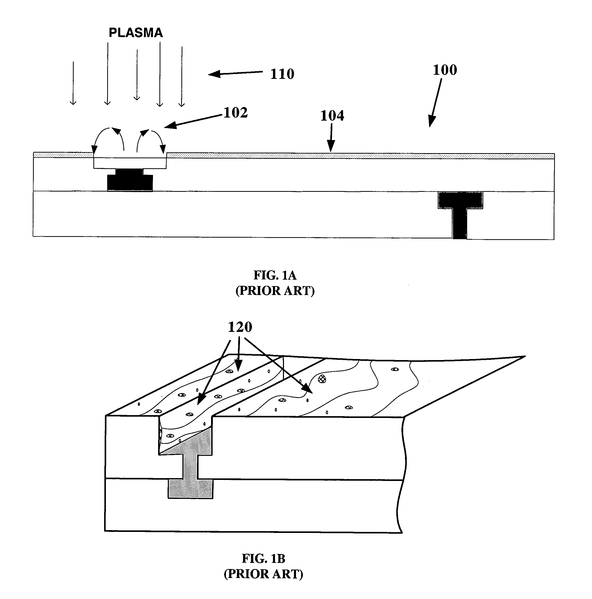
a technology of liquid meniscus and etching wafers, applied in the direction of cleaning with liquids, cleaning processes and apparatuses, chemistry apparatus and processes, etc., can solve the problems of reducing reliability or even failure of ic, contaminated wafers, and complex process of semiconductor chip fabrication

Inactive Publication Date: 2009-10-06
LAM RES CORP
View PDF9 Cites 7 Cited by
  • Summary
  • Abstract
  • Description
  • Claims
  • Application Information

AI Technical Summary

Benefits of technology

[0007]Broadly speaking, the present invention fills these needs by providing an improved cleaning method to removed contaminants from the surface of a wafer. It should be appreciated that the present invention can be implemented in numerous ways, including as a system, an apparatus and a method. Several inventive embodiments of the present invention are described below.
[0008]In one embodiment, a method for cleaning a semiconductor wafer is defined. A proximity head is provided which includes a plurality of source inlets and a plurality of source outlets. Next, the proximity head is defined in close proximity to a wafer surface. After the proximity head is defined in close proximity to the wafer surface, an oxidizer solution is applied through the plurality of source inlets to the wafer surface. The oxidizer solution forms an oxidized layer on one or more contaminant species on the wafer surface. The oxidizer solution is removed from the wafer surface through the plurality of source outlets. Then a cleaning solution is applied to the wafer surface through the plurality of source inlets. The cleaning solution is configured to substantially remove the oxidized layer along with the one or more contaminant species on the wafer surface. The cleaning solution is removed from the wafer surface through the plurality of source outlets.
[0009]In another embodiment, a method for cleaning a semiconductor wafer begins by applying to a wafer surface a first cleaning solution to remove one or more contaminant species on the wafer surface. The first cleaning solution is removed from the wafer surface along with at least some of the one or more contaminant species. Next, an oxidizer solution is applied to the wafer surface. The oxidizer solution forms an oxidized layer on remaining contaminant species. The oxidizer solution is removed from the wafer surface. Next, a second cleaning solution is applied to the wafer surface. The second cleaning solution is configured to substantially remove the oxidized layer along with the remaining contaminant species. The second cleaning solution is removed from the wafer surface.
[0010]In still another embodiment, a method for cleaning a semiconductor wafer is defined. A proximity head is provided which includes a plurality of source inlets and a plurality of source outlets. The proximity head is defined in close proximity to a wafer surface. Next, a first cleaning solution to remove one or more contaminant species on the wafer surface is applied through the plurality of source inlets to the wafer surface. The first cleaning solution is removed along with at least some of the one or more contaminant species from the wafer surface through the plurality of source outlets. Then, an oxidizer solution is applied through the plurality of source inlets to the wafer surface. The oxidizer solution forms an oxidized layer on remaining contaminant species. The oxidizer solution is removed through the plurality of source inlets. A second cleaning solution is applied through the plurality of source inlets to the wafer. The second cleaning solution is configured to substantially remove the oxidized layer along with the remaining contaminant species. The second cleaning solution is removed from the wafer surface through the plurality of source outlets.

Problems solved by technology

Semiconductor chip fabrication is a complicated process that involves a coordinated series of precise operations.
It is well known that during the various steps in these operations, the surfaces of the semiconductor substrate (i.e., semiconductor wafers) become contaminated with a layer of residue comprised of particulates, organic materials, metallic impurities (e.g. copper, aluminum, titanium, tungsten, etc.), and native oxides (e.g., silicon dioxide).
Removal of these contaminants is a vital step in producing ICs because contaminants on a wafer surface cause defects in the IC which result in decreased reliability or even failure of the IC.
However, these formulations are expensive to purchase in sufficient quantities for large scale wafer manufacturing.
Furthermore, these proprietary chemicals often take several minutes to effectively remove the contaminants on the wafer surface.
This delay can result in lower wafer output which adds to the expense of employing these formulations in the context of large-scale wafer manufacturing.
However, the amount of contamination that remains on the wafer surface remains unacceptably high unless long process times are provided to clean the wafer surface.
This is equally counterproductive to the goal of achieving high throughput wafer manufacture.

Method used


Image

  • Post etch wafer surface cleaning with liquid meniscus
  • Post etch wafer surface cleaning with liquid meniscus
  • Post etch wafer surface cleaning with liquid meniscus

Examples


Embodiment Construction

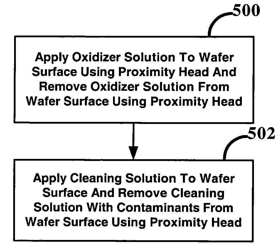
[0022]An invention is described for apparatuses, systems, and methods for cleaning the surface of a semiconductor substrate. It will be obvious, however, to one skilled in the art, that the present invention may be practiced without some or all of these specific details. In other instances, well known process operations have not been described in detail in order not to unnecessarily obscure the present invention.

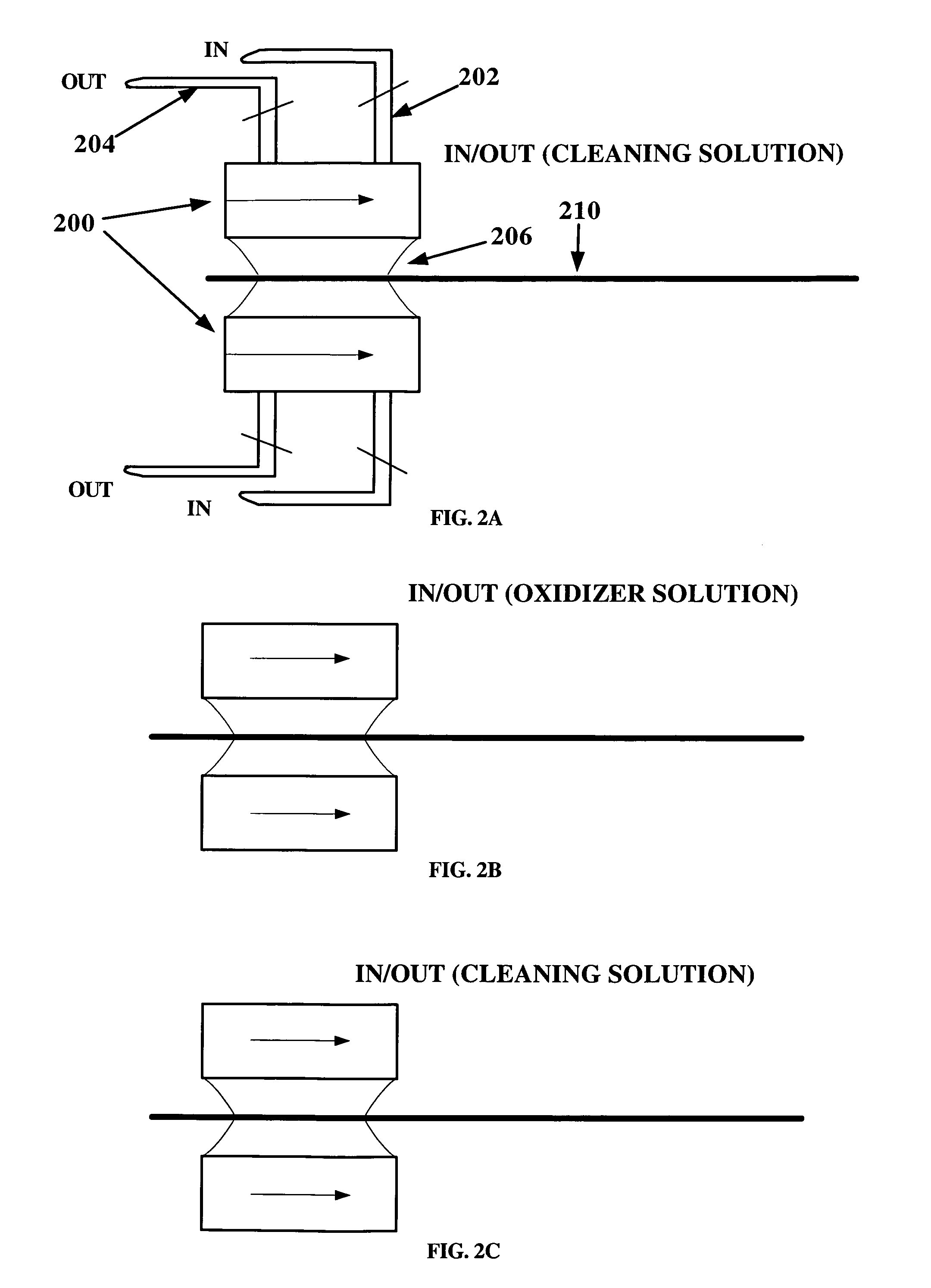
[0023]A semiconductor substrate can be made of any silicon-based material. In one exemplary embodiment, the substrate is a semiconductor wafer, which is a thin slice of semiconductor material, such as a silicon crystal, upon which microcircuits are constructed by diffusion and deposition of various materials. In this document, the terms semiconductor substrate and semiconductor wafer are used inter-changeably. What is disclosed by the embodiments herein is essentially a semiconductor substrate cleaning method that can be used with customized configurations of proximity heads...


PUM

PropertyMeasurementUnit
concentrationaaaaaaaaaa
areasaaaaaaaaaa
areaaaaaaaaaaa

Abstract

A method for cleaning the surface of a semiconductor wafer is disclosed. A first cleaning solution is applied to the wafer surface to remove contaminants on the wafer surface. The first cleaning solution is removed with some of the contaminants on the wafer surface. Next, an oxidizer solution is applied to the wafer surface. The oxidizer solution forms an oxidized layer on remaining contaminants. The oxidizer solution is removed and then a second cleaning solution is applied to the wafer surface. The second cleaning solution is removed from the wafer surface. The cleaning solution is configured to substantially remove the oxidized layer along with the remaining contaminants.

Description

CLAIM OF PRIORITY[0001]This is a continuation-in-part application claiming priority from U.S. patent application Ser. No. 10 / 261,839, filed Sep. 30, 2002, now Pat. No. 7,234,477, issued on Jun. 26, 2007, entitled “Method And Apparatus For Drying Semiconductor Wafer Surfaces Using A Plurality Of Inlets And Outlets Held In Close Proximity To The Wafer Surfaces” by John M. de Larios et al. The aforementioned patent is incorporated by reference in its entirety for all purposes.BACKGROUND[0002]Semiconductor chip fabrication is a complicated process that involves a coordinated series of precise operations. It is well known that during the various steps in these operations, the surfaces of the semiconductor substrate (i.e., semiconductor wafers) become contaminated with a layer of residue comprised of particulates, organic materials, metallic impurities (e.g. copper, aluminum, titanium, tungsten, etc.), and native oxides (e.g., silicon dioxide).[0003]An example of wafer contamination creat...

Claims


Application Information

Patent Timeline
Patent Type & Authority Patents(United States)
IPC IPC(8): B08B3/08C23G1/02H01L21/00
CPCH01L21/67028H01L21/67051H01L21/67034Y10S134/902B08B3/00H01L21/00H01L21/302H01L21/304
Inventor ZHU, JIYUN, SEOKMINWILCOXSON, MARKDE LARIOS, JOHN
Owner LAM RES CORP
Why Eureka
Try Eureka