Cleaning solution including aqueous ammonia solution, acetic acid and deionized water for integrated circuit devices and methods of cleaning integrated circuit devices using the same

Active Publication Date: 2005-09-20
SAMSUNG ELECTRONICS CO LTD
5 Cites 0 Cited by

AI-Extracted Technical Summary

Problems solved by technology

However, as the end product devices have become more and more miniaturized and complex, the cleanliness requirements may become increasingly more stringent so that the devices may function properly.
Therefore, the cleaning solution including the hydrogen chloride may not be desirable for cleaning an integrated circuit device having an exposed metal pattern.
Additionally in this process, the hydrogen peroxide solution may generate bubbles from oxyg...

Benefits of technology

[0015]Accordingly, embodiments of the present invention may pr...

Abstract

Cleaning solutions for integrated circuit devices and methods of cleaning integrated circuit devices using the same are disclosed. The cleaning solution includes about 30% aqueous ammonia solution, acetic acid by a volume percent higher then a volume percent of the aqueous ammonia solution, and deionized water by a volume percent higher then the volume percent of the acetic acid. Additionally, disclosed are methods wherein the cleaning solution is formed on integrated circuit substrates having an exposed metal pattern formed thereon, and further providing mega-sonic energy to the film of the cleaning solution.

Application Domain

Detergent mixture composition preparationElectrostatic cleaning +4

Technology Topic

IonAmmonium hydroxide +6

Image

  • Cleaning solution including aqueous ammonia solution, acetic acid and deionized water for integrated circuit devices and methods of cleaning integrated circuit devices using the same
  • Cleaning solution including aqueous ammonia solution, acetic acid and deionized water for integrated circuit devices and methods of cleaning integrated circuit devices using the same
  • Cleaning solution including aqueous ammonia solution, acetic acid and deionized water for integrated circuit devices and methods of cleaning integrated circuit devices using the same

Examples

  • Experimental program(19)

Example

EXAMPLE 1
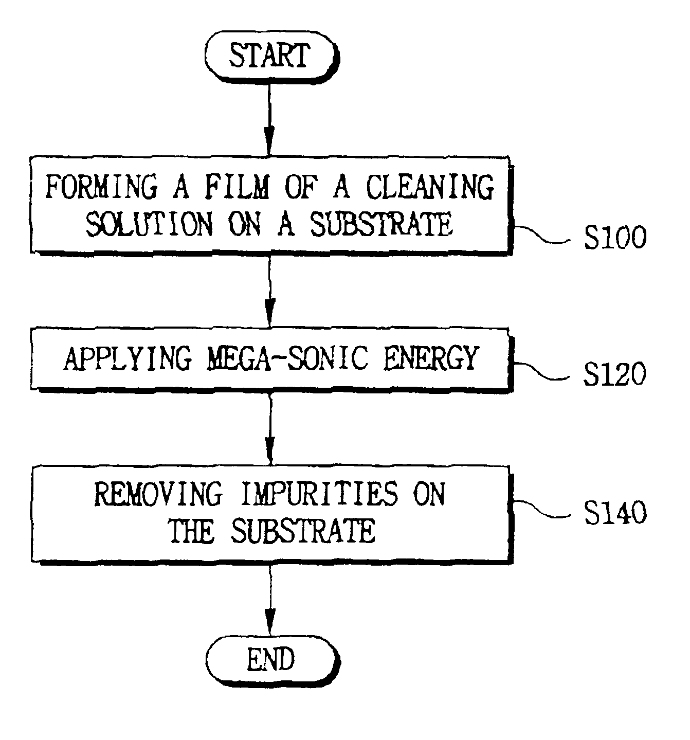
[0037]A cleaning solution including about 30% aqueous ammonia solution, acetic acid and deionized water was prepared. A volume ratio among the about 30% aqueous ammonia solution, the acetic acid and the deionized water was about 1:2:2,000. The cleaning solution was provided onto an integrated circuit substrate including exposed aluminum patterns while the integrated circuit substrate was rotated by a speed of about 20 rpm. At that time, the cleaning solution had a thickness of about 2 mm on the integrated circuit substrate. The cleaning solution was provided at a room temperature for about 30 seconds.

Example

EXAMPLE 2
[0038]A cleaning solution including about 30% aqueous ammonia solution, acetic acid and deionized water was prepared. A volume ratio among the about 30% aqueous ammonia solution, the acetic acid and the deionized water was about 1:2:4,000. The cleaning solution was provided onto an integrated circuit substrate including exposed aluminum patterns while the integrated circuit substrate was rotated at a speed of about 20 rpm. At that time, the cleaning solution had a thickness of about 2 mm on the integrated circuit substrate. The cleaning solution was provided at a room temperature for about 30 seconds.

Example

EXAMPLE 3
[0039]A cleaning solution including about 30% aqueous ammonia solution, acetic acid and deionized water was prepared. A volume ratio among the about 30% aqueous ammonia solution, the acetic acid and the deionized water was about 1:1:1,000. The cleaning solution was provided onto an integrated circuit substrate including exposed aluminum patterns while the integrated circuit substrate was rotated by a speed of about 20 rpm. At that time, the cleaning solution had a thickness of about 2 mm on the integrated circuit substrate. The cleaning solution was provided at a room temperature for about 30 seconds.

PUM

PropertyMeasurementUnit
Fraction0.3fraction
Thickness7.0E-4 ~ 0.0027m
Power10.0 ~ 100.0W

Description & Claims & Application Information

We can also present the details of the Description, Claims and Application information to help users get a comprehensive understanding of the technical details of the patent, such as background art, summary of invention, brief description of drawings, description of embodiments, and other original content. On the other hand, users can also determine the specific scope of protection of the technology through the list of claims; as well as understand the changes in the life cycle of the technology with the presentation of the patent timeline. Login to view more.
Why Eureka
Try Eureka