
Multi-standard data communication interface circuitry for programmable logic devices

Inactive Publication Date: 2009-10-06
ALTERA CORP
View PDF3 Cites 1 Cited by
  • Summary
  • Abstract
  • Description
  • Claims
  • Application Information

AI Technical Summary

Benefits of technology

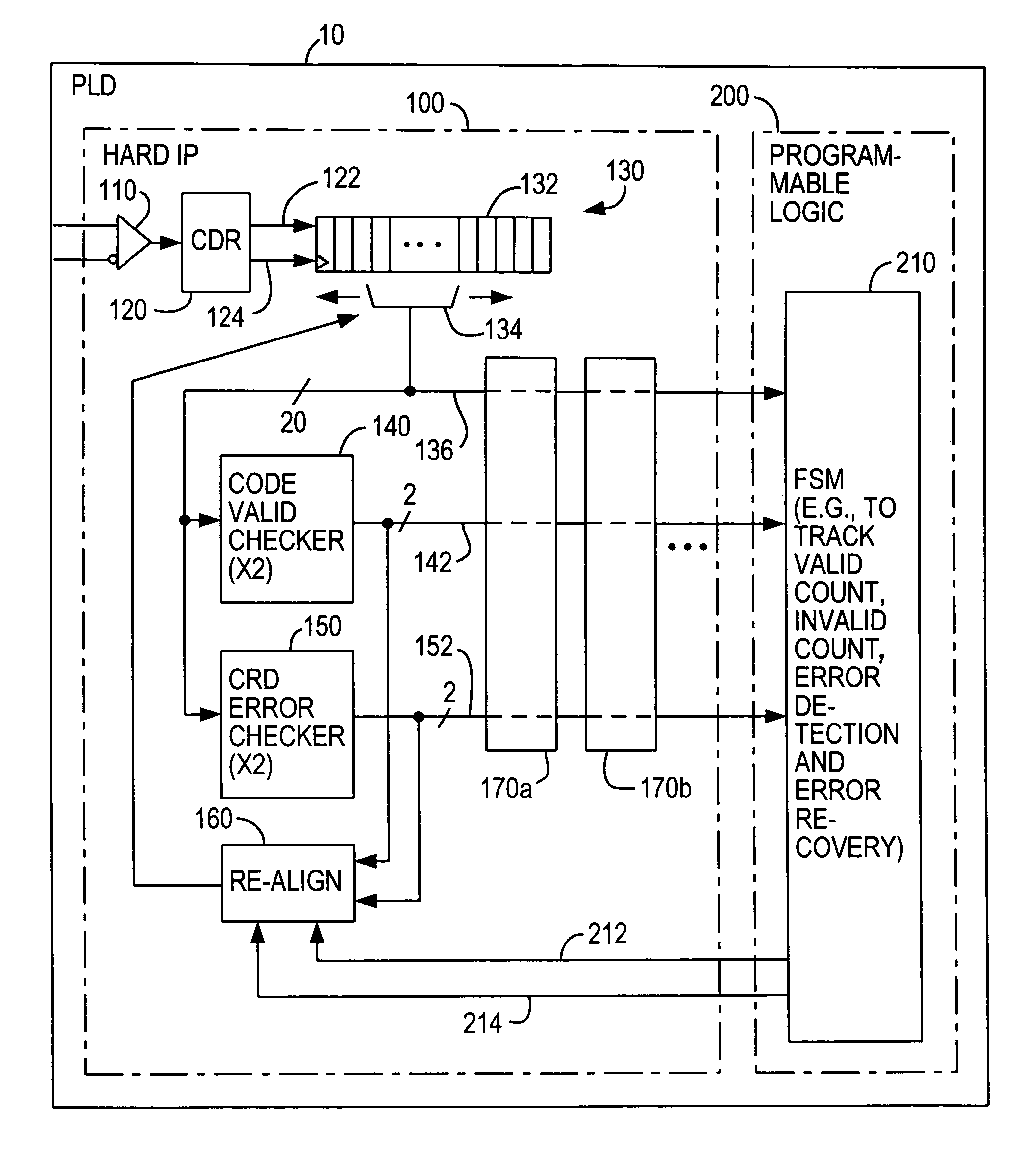
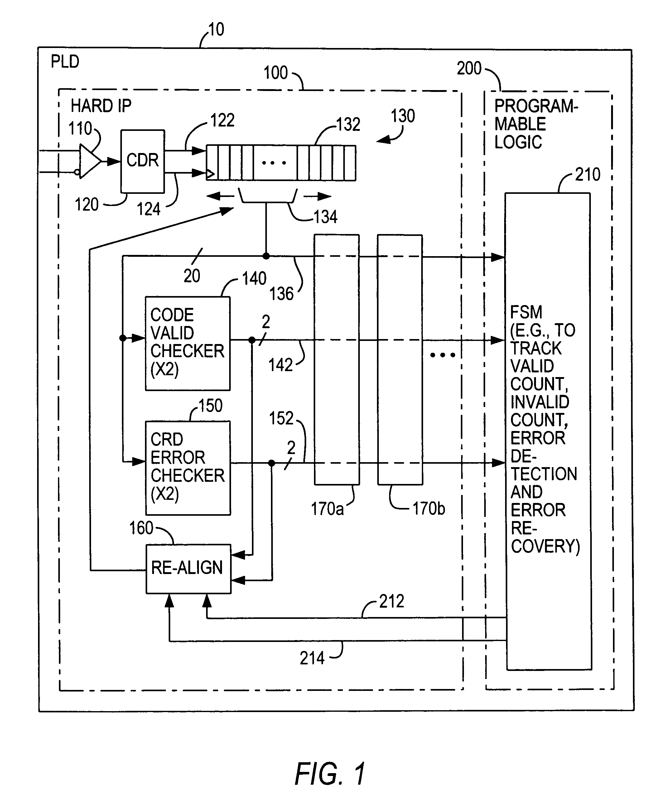
[0006]The aligned bytes and output signals of the hard IP circuitry performing checks of the aligned bytes as described in the preceding paragraph are applied to downstream circuitry. This downstream circuitry may include additional dedicated data processing circuitry in the hard IP portion of the PLD. The downstream circuitry also includes the programmable logic portion of the PLD. That programmable logic is typically configured (programmed) to perform tasks on the aligned bytes that tend to have relatively large variation among a wide range of communication protocols that can be implemented by the PLD. For example, these tasks typically include synchronizing the bytes in accordance with the data structure of whatever communication protocol is being implemented. As part of its tasks, the programmable logic may feed back to the hard IP signals for affecting how the bytes are being aligned in the hard IP. To increase the speed at which a change in byte alignment can be made, the programmable logic can enable the byte alignment circuitry in the hard IP to respond directly to code or CRD errors detected far upstream in the hard IP as described in the preceding paragraph. The hard IP preferably operates on two bytes at a time.

Problems solved by technology

This is made more difficult by both of the trends noted above, i.e., increased communication speed and increased number of possible communication protocols.
However, increased number of possible protocols suggests that a large amount of dedicated circuitry will be needed (to support the peculiarities of each possible protocol), but that much of that circuitry will be unused and therefore wasted when the PLD is used for only one or at most a few of the possible protocols.

Method used


Image

  • Multi-standard data communication interface circuitry for programmable logic devices
  • Multi-standard data communication interface circuitry for programmable logic devices
  • Multi-standard data communication interface circuitry for programmable logic devices

Examples


Embodiment Construction

[0010]In the illustrative embodiment shown in FIG. 1 the invention is implemented in a PLD 10. PLD 10 has two principal parts that are relevant to the invention. These are hard IP (intellectual property) part 100 and programmable logic part 200. Hard IP 100 includes circuitry that is at least partly hard-wired to perform particular, relatively high-level functions. Certain aspects of these functions may be programmable or otherwise variably controllable. But the basic type(s) of these functions is fixed. Another term for this type of circuitry is dedicated (i.e., because the circuitry is dedicated to performing particular functions and cannot be used for performing other functions).

[0011]Programmable logic 200 is traditionally the major part of a PLD. It is relatively general-purpose circuitry that can be programmed to perform any of a wide range of functions.

[0012]Hard IP 100 includes serial data signal input buffer circuitry 110 for receiving a serial data signal from a source ext...


PUM


Abstract

A programmable logic device includes a hard IP portion, which includes circuitry that is dedicated to receiving a high-speed serial data signal and performing certain basic functions related to byte alignment on that data signal, and a more general-purpose programmable logic portion. The programmable logic portion is used for such tasks as synchronizing the byte-aligned data in accordance with any one of a number of possible data communication protocols.

Description

[0001]This is a continuation of U.S. patent application Ser. No. 11 / 303,807, filed Dec. 15, 2005, which is hereby incorporated by reference herein in its entirety. This application also claims the benefit of U.S. provisional patent application 60 / 707,616 filed Aug. 12, 2005, which is also hereby incorporated by reference herein in its entirety.BACKGROUND OF THE INVENTION[0002]This invention relates to programmable logic devices (“PLDs”) or the like, and more particularly to PLD circuitry that facilitates use of the PLD to support any of many different data communication protocols, especially protocols that involve the use of one or more high-speed serial data streams.[0003]High-speed serial data communication is increasingly of interest, e.g., for signaling between various devices in a system such as integrated circuits on a printed circuit board. The speed at which such communication is desired is constantly increasing, and the known standards or protocols for such communication ar...

Claims


Application Information

Patent Timeline
IPC IPC(8): H03K19/173
CPCH03K19/17744H03K19/17732
Inventor XUE, NING
Owner ALTERA CORP
Learn More