Method for producing a device comprising a structure equipped with one or more microwires or nanowires based on a Si and Ge compound by germanium condensation

a technology of microwires and nanowires, applied in the field of transistors, can solve the problems of high substrate cost, difficult control of wire shape and precise position, and complex lithography implementation techniques,

Active Publication Date: 2009-10-13
COMMISSARIAT A LENERGIE ATOMIQUE ET AUX ENERGIES ALTERNATIVES
View PDF7 Cites 30 Cited by
  • Summary
  • Abstract
  • Description
  • Claims
  • Application Information

AI Technical Summary

Problems solved by technology

However, with such a method, it is difficult to control the shape of the wires and precisely position them.
This approach however requires the implementation of complex techniques of lithography, selective epitaxy and selective isotropic etching.
A disadvantage of transistors equipped with a channel formed in a germanium-based substrate is the high cost of the substrate.
In addition, it is very difficult to produce channels with germanium or a SiGe alloy rich in Ge having a good crystalline quality by epitaxy.
By way of example, it is currently difficult to produce good metallic contacts on source and drain zones constituted by a SiGe material with a Ge composition higher than 30%.
The problem to be solved is that of finding a new method for producing a microelectronic device equipped with Si1−zGez-based semiconductors based on having a high germanium concentration.

Method used


Image

  • Method for producing a device comprising a structure equipped with one or more microwires or nanowires based on a Si and Ge compound by germanium condensation
  • Method for producing a device comprising a structure equipped with one or more microwires or nanowires based on a Si and Ge compound by germanium condensation
  • Method for producing a device comprising a structure equipped with one or more microwires or nanowires based on a Si and Ge compound by germanium condensation

Examples


Embodiment Construction

[0009]This invention is intended to overcome the disadvantages mentioned above and to produce a “wire”-type channel structure made of Ge or an alloy of silicon and Ge of micro or nanometric size on an insulator by germanium condensation.

[0010]The invention relates in particular to the production of a microelectronic device comprising one or more Si1−zGez-based semiconductor wire(s) (with 0

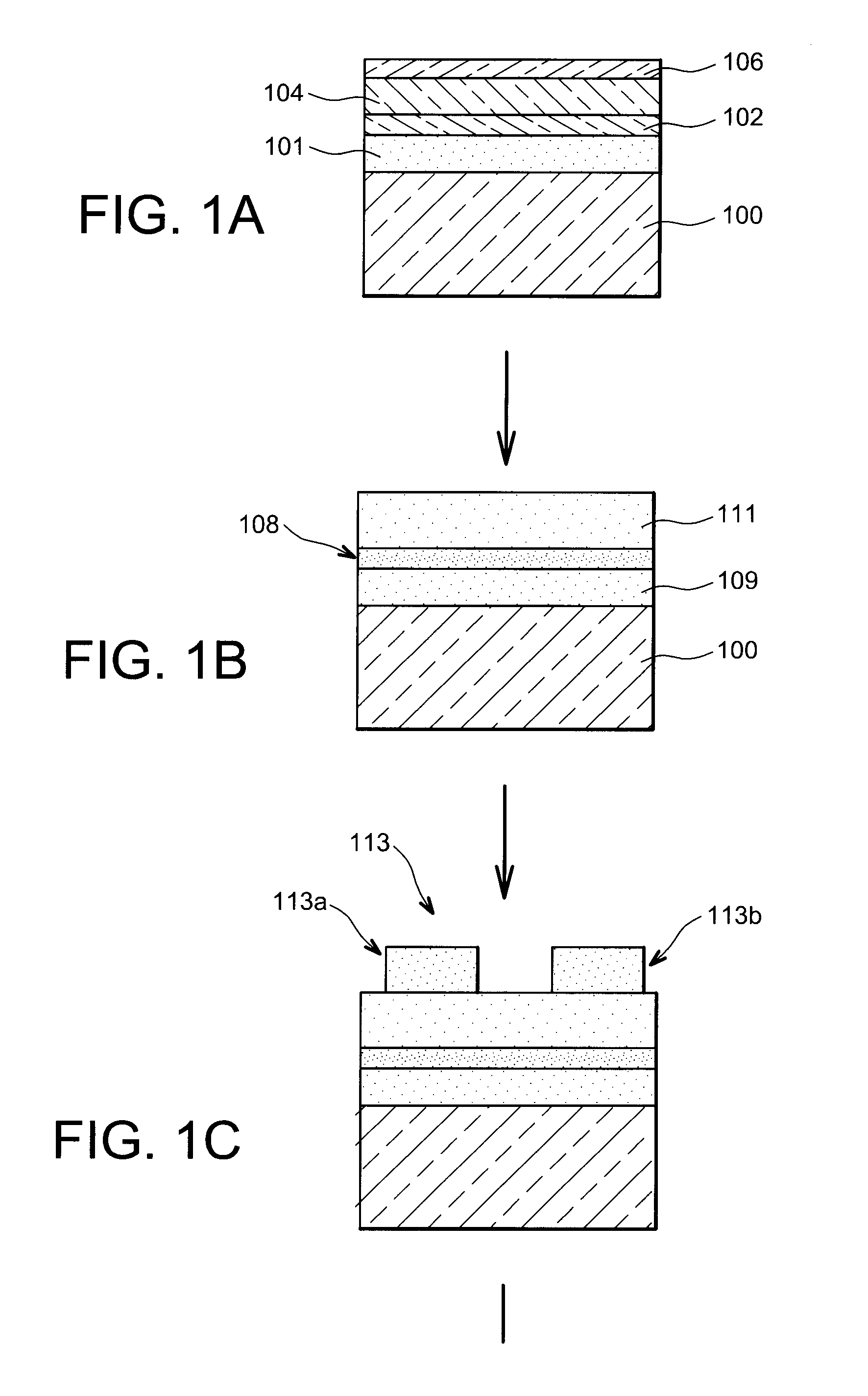
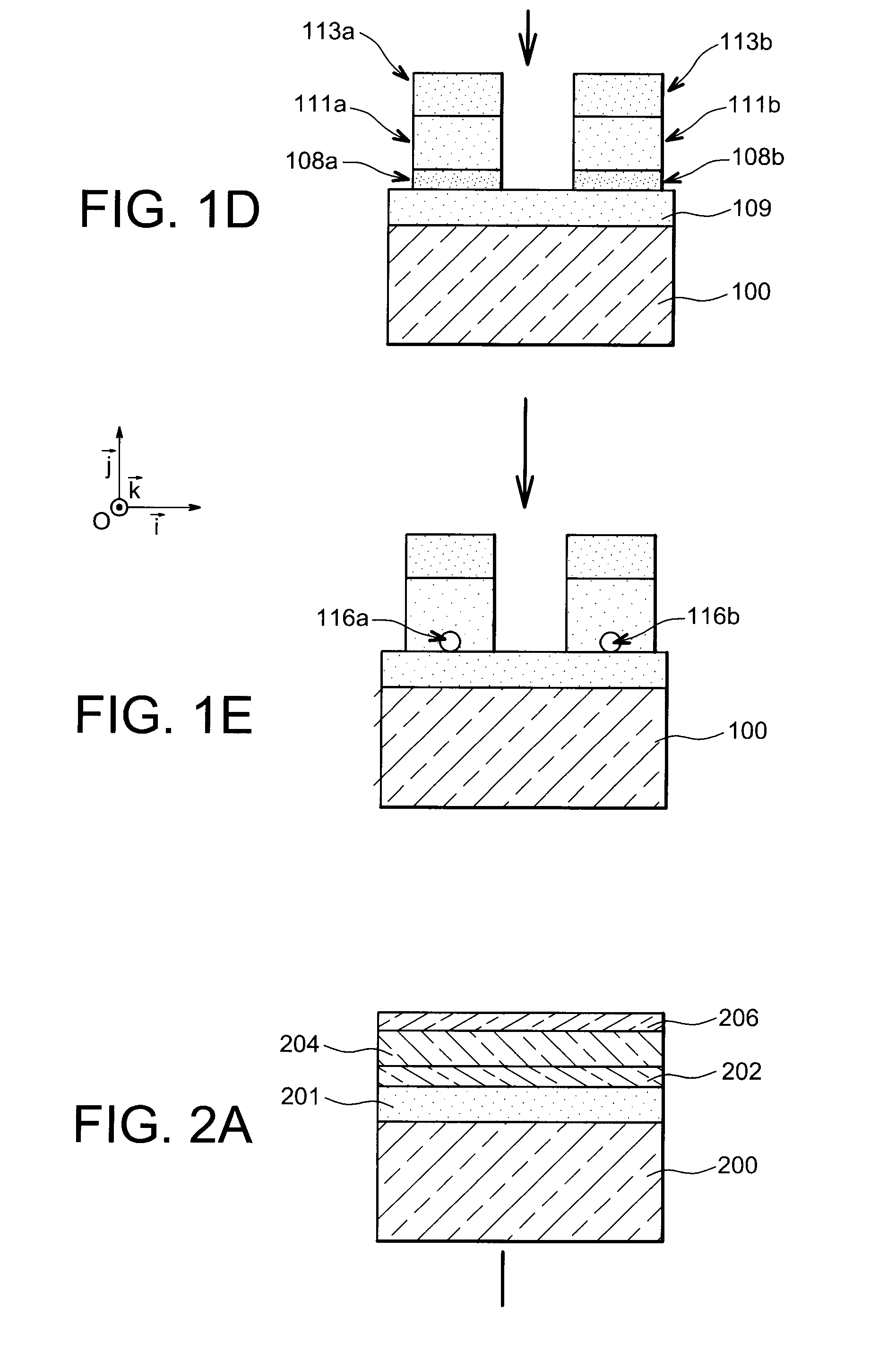
[0011]a) thermal oxidation of at least a portion of a Si1−xGex-based semiconductor layer (with 01−yGey-based semiconductor zone (with 0

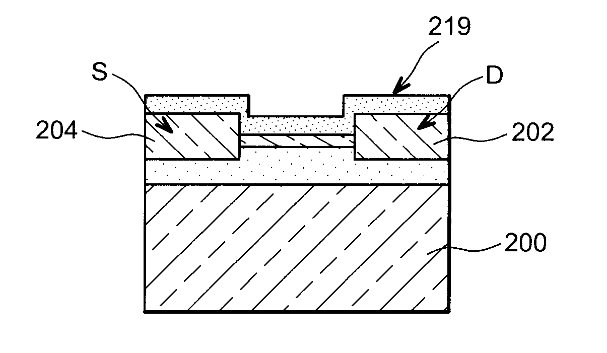
[0012]b) lateral thermal oxidation of the sides of one or more so-called semiconductor “connection” blocks from said Si1−yGey-based semiconductor zone and connecting a semiconductor block intended to form a transistor source region and another block intended to form a transistor drain region so as to reduce the semiconductor connection blocks in at least one direction parallel to the main plane of the support and to form o...


PUM


Abstract

A method for producing a microelectronic device having one or more Si1−zGez based semiconductor wire(s) (with 0<z≦1), including:a) thermal oxidation of at least a portion of a Si1−xGex-based semiconductor layer (with 0<x<1) resting on a support, so as to form at least one Si1−yGey-based semiconductor zone (with 0<y<1 and x<y),b) lateral thermal oxidation of the sides of one or more so-called semiconductor connection blocks from the Si1−yGey-based semiconductor zone and connecting a semiconductor block intended to form a transistor source region and another block intended to form a transistor drain region so as to reduce the semiconductor connection blocks in at least one direction parallel to the main plane of the support and to form one or more Si1−zGez-based semiconductor wire(s) (with 0<y<1 and y<z).

Description

TECHNICAL FIELD[0001]This invention relates to a method for producing an improved microelectronic device in which Si1−zGez-based semiconductor nanowires (with z>0) are formed, using at least one first step of thermal oxidation of one or more semiconductor zones based on a silicon and germanium compound, and at least one step of lateral thermal oxidation of one or more semiconductor zones based on another silicon and germanium compound resulting from the first oxidation.[0002]This invention relates more specifically to transistors, and is intended to present a transistor equipped in particular with a channel or multi-channel structure in the form of one or more Si1−zGez-based nanowire(s), connecting a semiconductor zone intended to act as a drain region. Such a structure can be adapted to so-called “embedded” gate structures. The problem to be solved is that of finding a new method for producing a microelectronic device comprising a structure equipped with one or more semiconducto...

Claims


Application Information

Patent Timeline
Patent Type & Authority Patents(United States)
IPC IPC(8): H01L21/331
CPCB82Y10/00H01L29/0665H01L29/0673H01L29/78696H01L29/161H01L29/775H01L29/78684H01L29/1033
Inventor DAMLENCOURT, JEAN-FRANCOIS
Owner COMMISSARIAT A LENERGIE ATOMIQUE ET AUX ENERGIES ALTERNATIVES
Why Eureka
Try Eureka