Band gap reference voltage generation circuit

a reference voltage and generation circuit technology, applied in the direction of electric variable regulation, process and machine control, instruments, etc., can solve the problems of unstable factor of band gap reference voltage generation circuit, inability to use conventional reference voltage generation circuit as reference voltage circuit, and significant influence on production yield, so as to reduce wake up time and remove output voltage rf noise

Inactive Publication Date: 2009-10-13
TESSERA ADVANCED TECH
View PDF8 Cites 11 Cited by
  • Summary
  • Abstract
  • Description
  • Claims
  • Application Information

AI Technical Summary

Benefits of technology

[0028]The present invention has been made to solve the above problem occurring in the prior art, and therefore, consistent with the present invention, there is provided a band gap reference voltage generation circuit capable of reducing wake up time during transition from an idle mode to a normal mode and further capable of removing output voltage RF noise.
[0030]The band gap reference voltage generation circuit may further include a noise filter circuit connected to the power source voltage, the base voltage, and the first node to remove the RF noise of the output voltage of the first node and to output the output voltage to the output terminal.

Problems solved by technology

However, the band gap reference voltage generation circuit has unstable factors mainly caused by changes in the temperature or process conditions.
However, when a change in the manufacturing process exceeds process mismatch statistical data provided by a foundry industry, production yield is significantly affected.
However, since the conventional reference voltage generation circuit outputs a reference voltage of about 0.4V when the two input transistors in operation amplifier 10 are realized in a process having mismatch B no less than 0.11%, the conventional reference voltage generation circuit cannot be used as a reference voltage circuit.

Method used


Image

  • Band gap reference voltage generation circuit
  • Band gap reference voltage generation circuit
  • Band gap reference voltage generation circuit

Examples


Embodiment Construction

[0039]A reference voltage generating circuit consistent with the present invention will be described with reference to the attached drawing.

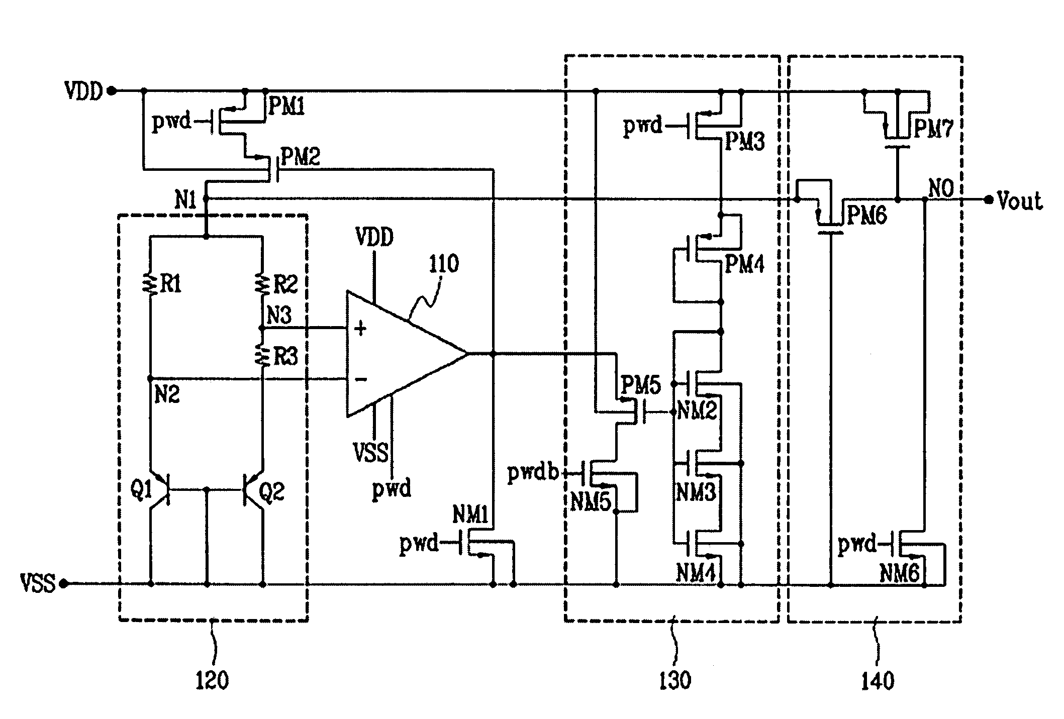
[0040]FIG. 3 is a circuit illustrating a band gap reference voltage generation circuit consistent with the present invention.

[0041]Referring to FIG. 3, a reference voltage generation circuit according to an embodiment of the present invention includes an operation amplifier 110 for outputting a uniform voltage in accordance with a reference voltage input to an inversion terminal (−) and a non-inversion terminal (+); a first PMOS transistor PM1 for outputting a power source voltage VDD in accordance with a power down signal pwd; a second PMOS transistor PM2 for outputting bias current corresponding to the output voltage from operation amplifier 110 using the output voltage from first PMOS transistor PM1; a reference voltage circuit 120 for supplying the reference voltage to inversion terminal (−) and non-inversion terminal (+) of operation amplif...


PUM


Abstract

There is provided a band gap reference voltage generation circuit capable of reducing wake up time during transition from an idle mode to a normal mode and further capable of removing the RF noise of an output voltage. The band gap reference voltage generation circuit includes an operation amplifier for outputting a uniform voltage in accordance with a reference voltage input to an inversion terminal and a non-inversion terminal; a first-type first transistor for outputting a power source voltage in accordance a power down signal; a first-type second transistor for outputting bias current corresponding to an output voltage from the operation amplifier using an output voltage from the first-type first transistor; a reference voltage circuit for supplying a reference voltage to the inversion terminal and the non-inversion terminal using the bias current; a second-type first transistor different from the first-type first transistor for supplying a base voltage to the output port of the operation amplifier in accordance with the power down signal; a start up circuit for driving the entire circuit during power up; a first node between the second-type second transistor and the reference voltage circuit; and an output terminal connected to the first node.

Description

RELATED APPLICATION[0001]This application claims the benefit of Korean Application No. 10-2005-0132609, filed on Dec. 28, 2005, which is incorporated by reference herein in its entirety.BACKGROUND[0002]1. Technical Field[0003]The present invention relates to a band gap reference voltage generation circuit. More specifically, the present invention relates to a band gap reference voltage generation circuit capable of reducing wake up time during the transition from an idle mode to a normal mode and further capable of removing radio frequency (RF) noise of an output voltage.[0004]2. Description of the Related Art[0005]In a semiconductor integrated circuit, stability of an internal operation voltage is very important to secure the reliability of a semiconductor device. That is, even if an external power source voltage changes, such a change must not exert influence upon the integrated circuit. The devices must perform their unique functions in a stable manner. To this end, a band gap re...

Claims


Application Information

Patent Timeline
Patent Type & Authority Patents(United States)
IPC IPC(8): G05F3/02
CPCG05F3/30G05F3/265
Inventor JO, EUN SANG
Owner TESSERA ADVANCED TECH
Why Eureka
Try Eureka