

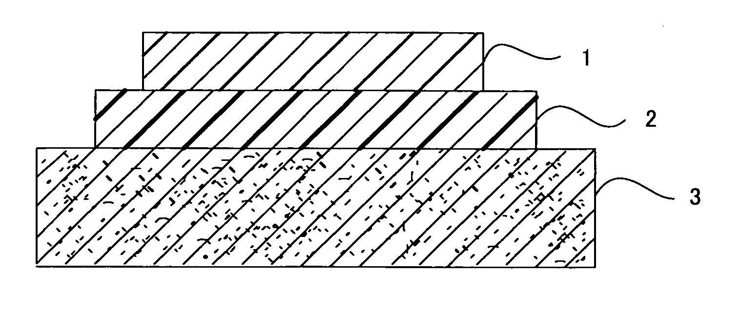
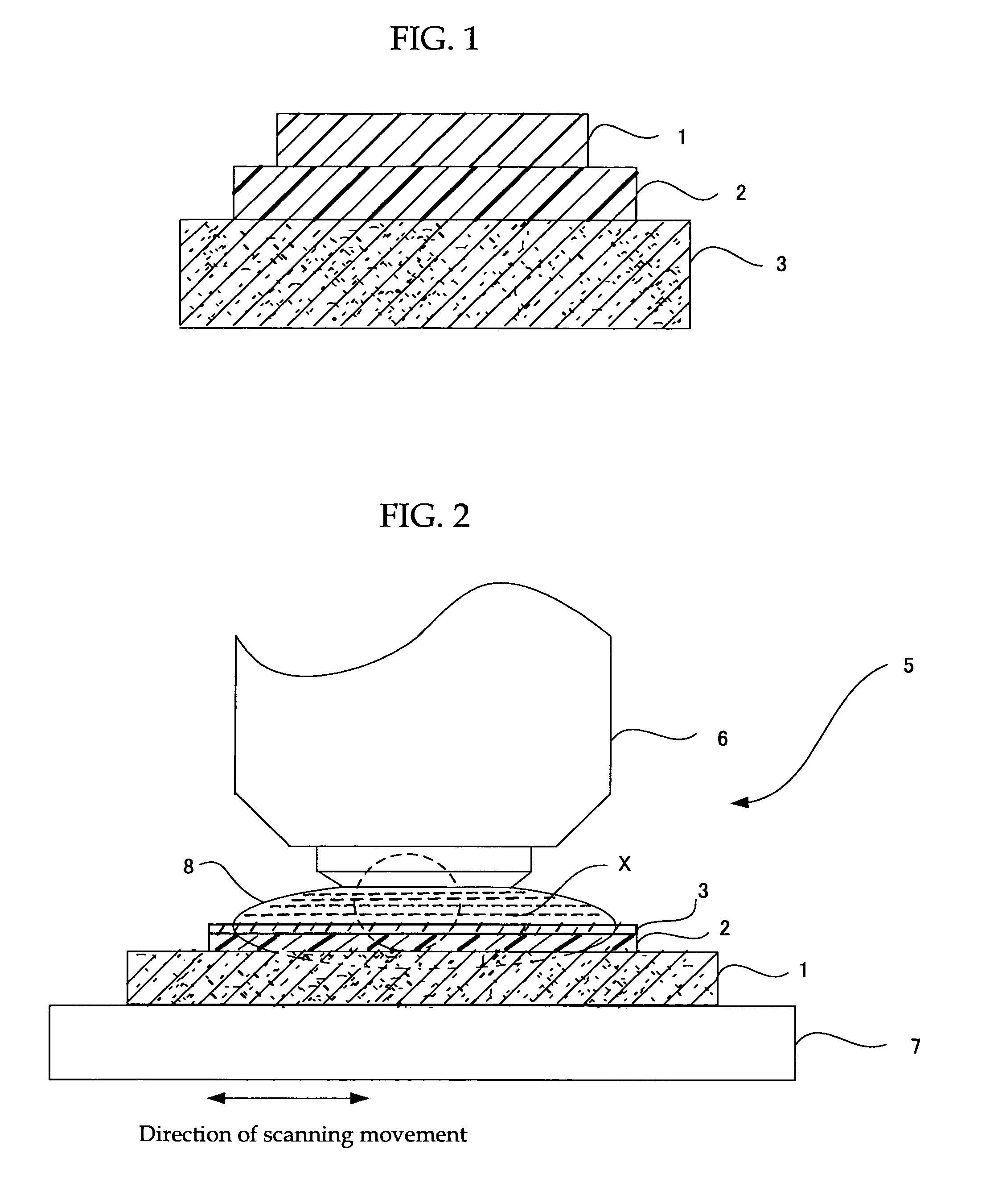
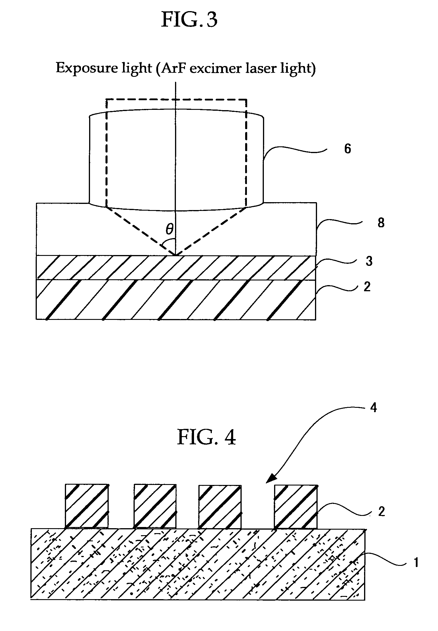
Resist cover film-forming material, process for forming resist pattern, semiconductor device and process for manufacturing the same
a technology of resist film and resist pattern, which is applied in the direction of photosensitive materials, instruments, photomechanical equipment, etc., can solve the problems of non-reactive light and inability to improve so as to prevent the intrinsic resist performance of the resist film from being impaired, the effect of efficient protection
- Summary
- Abstract
- Description
- Claims
- Application Information
AI Technical Summary
Benefits of technology
Problems solved by technology
Method used
Image

Examples
example 1
—Preparation of Resist Cover Film-Forming Material—
[0123]The resin having adamantane as the alicyclic skeleton at the side chains was synthesized as follows.
[0124]To an egg plant type flask, 2 g of methyl acrylate and 19.2 g of adamantyl acrylate were poured, and then 40 mL of tetrahydrofuran and 1.9 g of 2,2′-azobis-(isobutylonitrile)(AIBN) were added, and the solution was sufficiently substituted by nitrogen. The flask was soaked in an oil bath of 60° C. in nitrogen atmosphere to perform a reaction for 10 hours. The resultant solution was allowed to warm to the room temperature, and slowly delivered by drops into 1 L of methanol to obtain a white precipitate. The precipitate was filtrated through a glass filter and dissolved in tetrahydrofuran to precipitate in methanol to thereby purify the precipitate, and the process was repeatedly performed three times. The obtained resin was dried in a vacuum oven at a temperature of 40° C. for 20 hours to thereby obtain 15.3 g of a resin (we...
example 2
—Preparation of Resist Cover Film-Forming Material—
[0127]A resin having norbornane at the main chain and adamantane at the side chains respectively as the alicyclic skeleton was synthesized as follows.
[0128]To an egg plant type flask, 2 g of 5-norbornane-2-ol, 1.78 g of maleic anhydride, and 0.94 g of adamantyl acrylate were poured, and then 15 mL of anhydrous dioxane and 1 g of AIBN were added, and the solution was sufficiently substituted by nitrogen. The flask was soaked in an oil bath of 80° C. in nitrogen atmosphere to perform a reaction for 10 hours. The resultant solution was allowed to warm to the room temperature, and slowly delivered by drops into 1 L of hexane to obtain a white precipitate. The precipitate was filtrated through a glass filter and dissolved in dioxane to precipitate in methanol to thereby purify the precipitate, and the process was repeatedly performed three times. The obtained resin was dried in a vacuum oven at a temperature of 40° C. for 20 hours to the...
example 3
—Preparation of Resist Cover Film-Forming Material—
[0131]A resin having norbornane and cyclohexane respectively side chains as the alicyclic skeleton was synthesized as follows.
[0132]To an egg plant type flask, 2 g of 2-norbornile methacrylate, 1.49 g of cyclohexyl methacrylate, and 0.38 g of methacrylic acid were poured, and then 10 mL of tetrahydrofuran and 0.4 g of AIBN were added, and the solution was sufficiently substituted by nitrogen. The solution was soaked in an oil bath of 60° C. in nitrogen atmosphere to perform a reaction for 10 hours. The resultant solution was allowed to warm to the room temperature, and slowly delivered by drops into 1 L of methanol to obtain a white precipitate. The precipitate was filtrated through a glass filter and dissolved in tetrahydrofuran to precipitate in methanol to thereby purify the precipitate, and the process was repeatedly performed three times. The obtained resin was dried in a vacuum oven at a temperature of 40° C. for 20 hours to t...
PUM
| Property | Measurement | Unit |
|---|---|---|
| thickness | aaaaa | aaaaa |
| wavelength | aaaaa | aaaaa |
| refractive index | aaaaa | aaaaa |
Abstract
Description
Claims
Application Information