

Method and template for physical-memory allocation for implementing an in-system memory test
a technology of physical memory and in-system memory, applied in the field of memory system testing, can solve the problems of memory testing becoming even more critical, memory system becoming more and more susceptible to failure, and certain failure mechanisms,
- Summary
- Abstract
- Description
- Claims
- Application Information
AI Technical Summary
Benefits of technology
Problems solved by technology
Method used
Image

Examples
Embodiment Construction
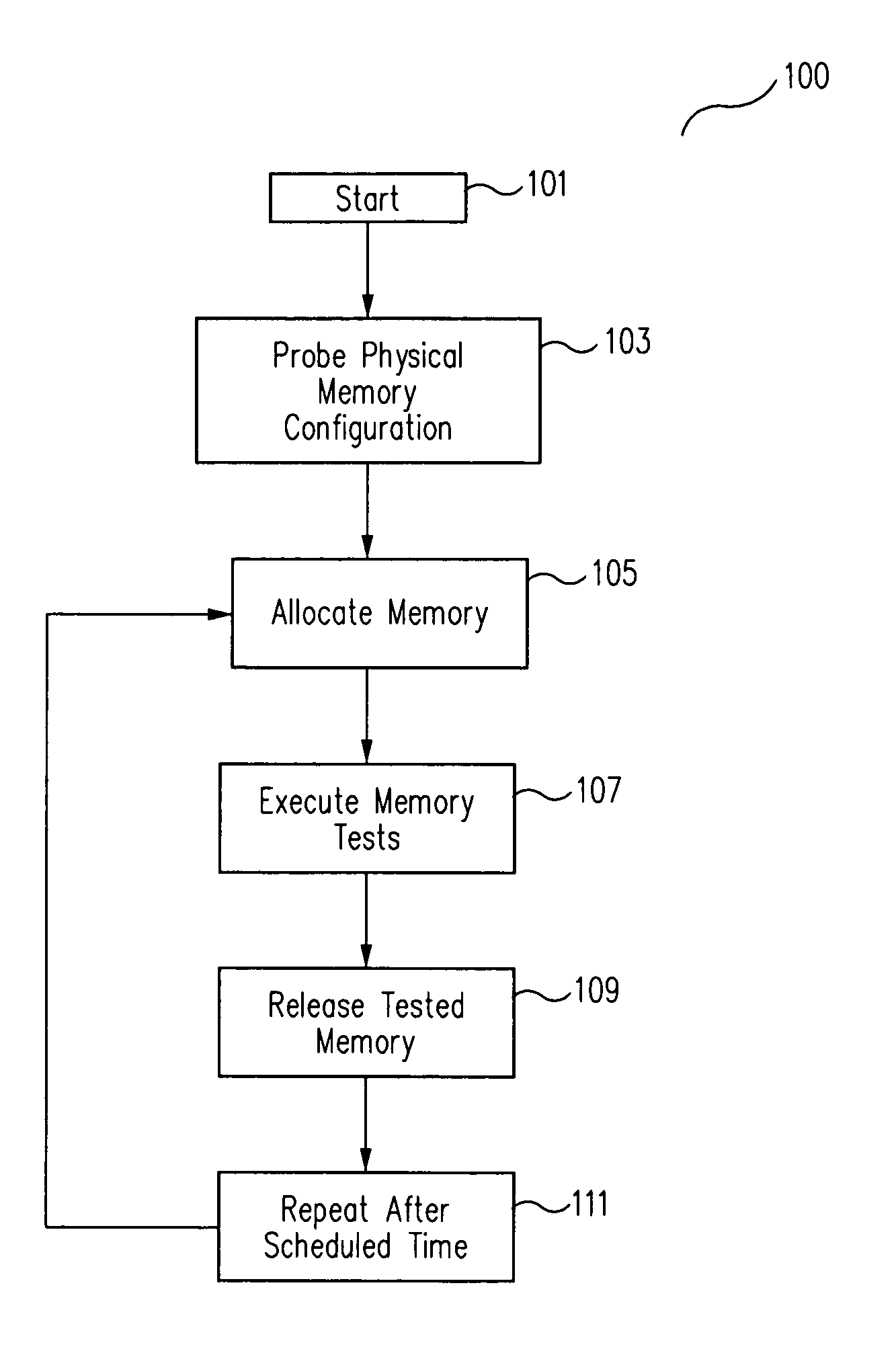
[0025]In accordance with one embodiment of the invention, an in-system memory testing method (100 in FIG. 1) is capable of testing system memory in both offline and online environments, without imposing any additional hardware requirements or significantly effecting computer or memory system performance.
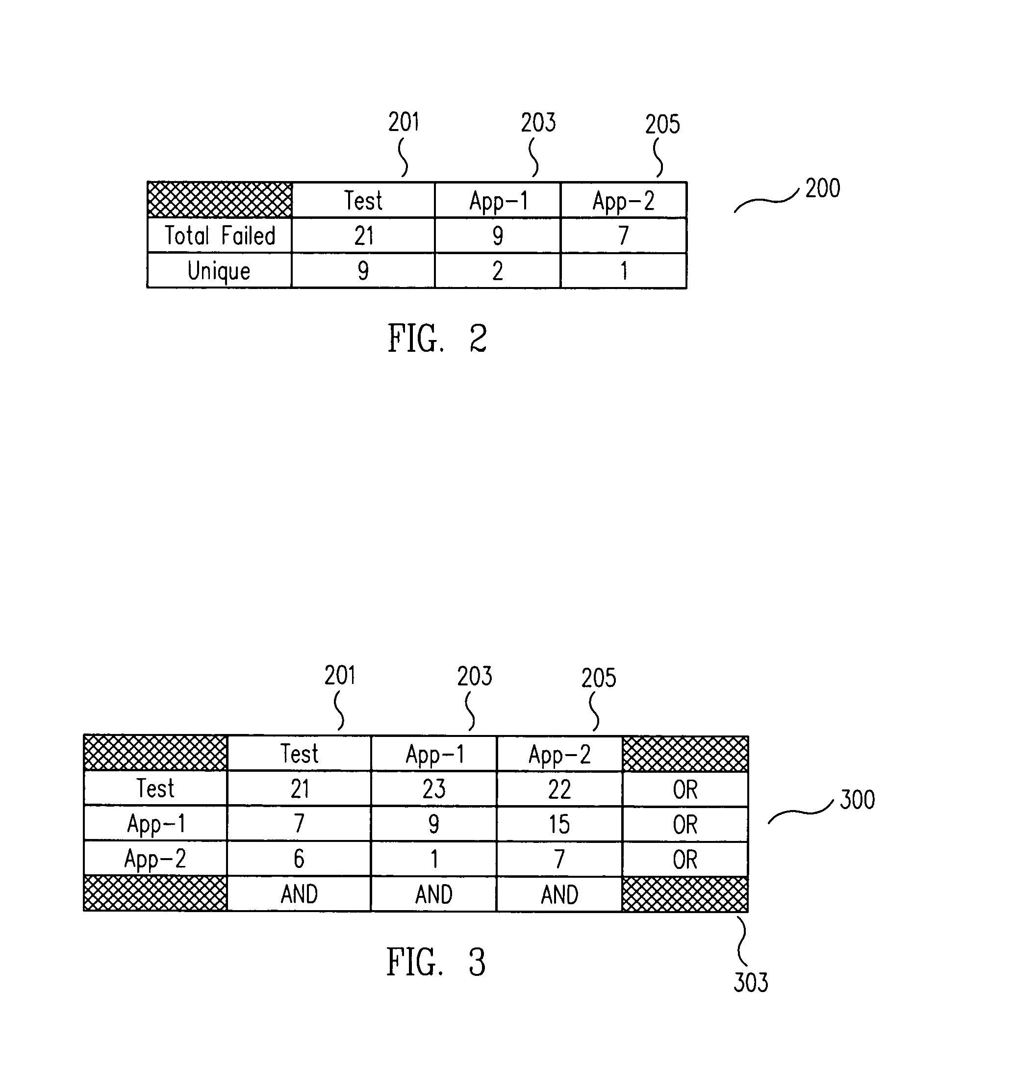
[0026]According to one embodiment of the invention, an in-system memory testing method includes transparently selecting and “stealing” a portion of physical memory from the system for testing (105 in FIG. 1), then running any one of numerous known memory system tests on the selected portion of memory (107 in FIG. 1), and then inserting the selected, and now tested, portion of physical memory back into the memory system for normal application use (109 in FIG. 1). Experimental results (FIGS. 2, 3, 4, 5 and 6) show that implementation of one embodiment of the in-system memory testing method of the invention can significantly improve the computer system's ability to proactively detect an...
PUM
 Abstract
Description
Claims
Application Information