Focused ion beam system and a method of sample preparation and observation

a focused ion beam and sample technology, applied in the field of focused ion beams, can solve the problems of difficult to apply to abnormal or deficient portions whose contour is difficult to predict, and become increasingly difficult to identify processing positions with the resolution of optical microscopes. achieve the effect of accurate setting and facilitation of image superposition

Inactive Publication Date: 2009-11-03
HITACHI HIGH-TECH CORP
View PDF9 Cites 27 Cited by
  • Summary
  • Abstract
  • Description
  • Claims
  • Application Information

AI Technical Summary

Benefits of technology

[0008]It is therefore an object of the invention to provide a focused ion beam system capable of acquiring surface structure information, internal structure information, and internal composition information simultaneously from the same field of view of the sample. It is another object of the invention to provide a method of sample preparation and observation whereby a sample processing position can be accurately set based on information about the structure and composition of a sample that is acquired from multiple directions using the aforementioned focused ion beam system.
[0009]In accordance with the invention, a focused ion beam system includes: a detector for detecting a secondary electron image based on scanning electron or scanning ion excitation as a detector for obtaining sample surface structure information; a transmission electron detector as a detector for obtaining sample internal structure information; and an energy dispersive X-ray spectroscope or an electron energy loss spectroscope as a detector for obtaining sample composition information. In order to observe the sample from multiple directions, a stub is used that has the sample rotating and tilting functions. Magnification correction between scanning electrons and scanning ions is carried out by comparing a secondary electron image based on scanning electron excitation with a secondary electron image based on scanning ion excitation, both images providing surface structure information about the sample. Superposition of images is facilitated by providing a marking that can be recognized in any observation mode and from any observation direction.

Problems solved by technology

Nowadays, however, there are semiconductor materials that contain 9 to 10 layers of wiring, and in some cases it is difficult to identify a processing position even by the aforementioned method whereby an image obtained by a separate method is superposed on the material.
And now that semiconductor production lines with 70 nm nodes are being established, it is becoming increasingly difficult to identify processing positions with the resolution of an optical microscope.
In addition, while CAD information can be applied to semiconductor materials that are manufactured according to design, it cannot be applied to abnormal or deficient portions whose contour is difficult to predict.

Method used


Image

  • Focused ion beam system and a method of sample preparation and observation
  • Focused ion beam system and a method of sample preparation and observation
  • Focused ion beam system and a method of sample preparation and observation

Examples


Embodiment Construction

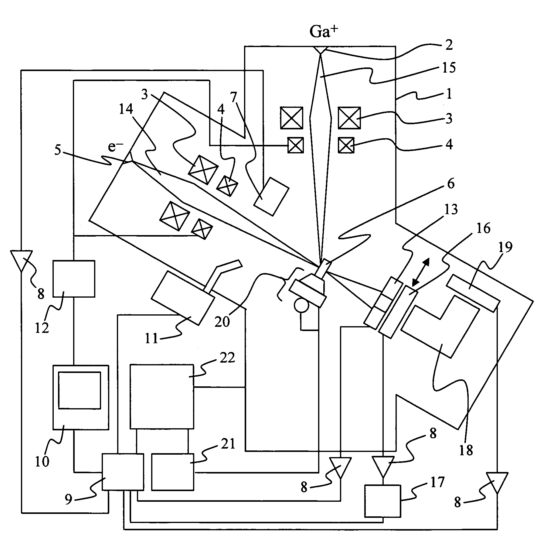
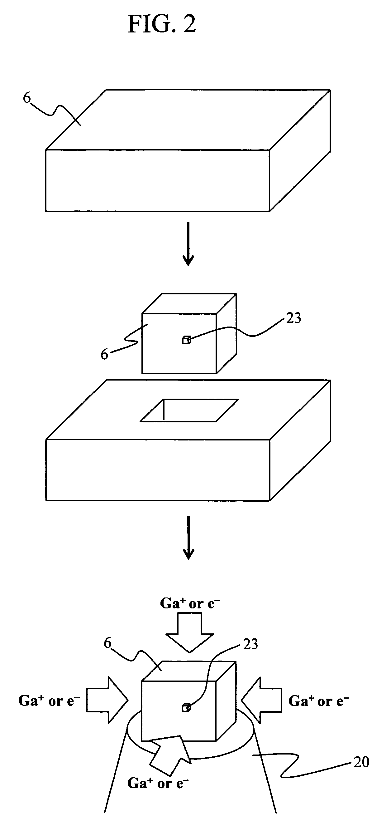
[0016]In the following, preferred embodiments of the focused ion beam system and method of sample preparation and observation according to the invention will be described with reference to the drawings. FIGS. 1 to 5 show the embodiments of the invention, throughout which similar parts having basically identical structure or operation are designated with similar reference signs.

[0017]In the focused ion beam system according to each of the embodiments, surface structure information, internal structure information, and internal composition information can be simultaneously acquired from the same field of view of the sample. The system includes a stub that has a rotating function and an tilting function, allowing the sample to be observed from multiple directions. The sample is presumed to have such a thickness as to allow the detection of transmission electrons. In a case where the acquisition of the sample structure and composition information and focused ion beam processing are carri...


PUM

PropertyMeasurementUnit
surface structureaaaaaaaaaa
internal structureaaaaaaaaaa
internal compositionaaaaaaaaaa

Abstract

A focused ion beam system capable of acquiring surface structure information, internal structure information, and internal composition information about a sample simultaneously from the same field of view of the sample. A method of sample preparation and observation employs such focused ion beam system to accurately set a sample processing position based on information about the structure and composition of the sample acquired from multiple directions of the sample, and to process and observe the sample. The system includes, in order to acquire the sample structure and composition information simultaneously, a secondary electron detector, a transmission electron detector, and an energy dispersive X-ray spectroscope or an electron energy loss spectroscope, and employs a stub having the sample rotating and tilting function. The method includes a marking process.

Description

BACKGROUND OF THE INVENTION[0001]1. Field of the Invention[0002]The present invention relates to focused ion beams, and particularly to a focused ion beam system capable of acquiring surface structure information, internal structure information, and internal composition information about a sample simultaneously. The invention also relates to methods of sample preparation and observation whereby the acquisition of such sample structure and composition information and focused ion beam processing are carried out using a plurality of devices.[0003]2. Background Art[0004]As the semiconductor devices become smaller and smaller in size, the electron microscope has become an indispensable tool for structural analysis. It has also become indispensable to use focused ion beam processing for the preparation of a sample for the observation of an electron microscope image. Focused ion beam processing generally involves capturing a scanning ion microscope (SIM) image and designating a position to...

Claims


Application Information

Patent Timeline
Patent Type & Authority Patents(United States)
IPC IPC(8): H01J37/26G01N23/22
CPCH01J37/3005H01J37/3056H01J2237/31745H01J2237/2516
Inventor SUZUKI, YUYAKAMINO, TAKEOYAGUCHI, TOSHIEKONNO, MITSURUOHNISHI, TSUYOSHI
Owner HITACHI HIGH-TECH CORP
Why Eureka
Try Eureka