Optical signal switching device for use in an optical protection network

a technology of optical protection network and optical signal switching device, which is applied in the field of communication nodes, can solve the problems of increased installation cost of optical network, increased cost of optical transmission device, and inevitable increase of optical transmission device cost, and achieves low cost and high reliability of optical network system

Active Publication Date: 2009-11-03
NEC CORP
View PDF23 Cites 12 Cited by
  • Summary
  • Abstract
  • Description
  • Claims
  • Application Information

AI Technical Summary

Benefits of technology

[0076]With the above configurations, if the failure occurs in any of optical fiber transmission lines, the switching device does switching so that the optical signal begins to be transmitted through another optical fiber transmission in which no failure has occurred and, therefore, installation of a communication line for standby use and of an optical si...

Problems solved by technology

Hei 4-334135, many optical fiber transmission lines have to be installed, thus causing increased costs for the installation of the optical network.
Moreover, in the case of providing service using a dark fiber, its usage charge is costly.
Hei 4-334135, increased costs for the optical transmission device are inevitable due to the many required optical components.
An optical signal transmitting device and an optical signal receiving device that can provide a transmission speed exceeding 10 G bps, in particular, are very costly and large in size, which causes high costs for the optical transmission device.
Moreover, since component...

Method used


Image

  • Optical signal switching device for use in an optical protection network
  • Optical signal switching device for use in an optical protection network
  • Optical signal switching device for use in an optical protection network

Examples


first embodiment

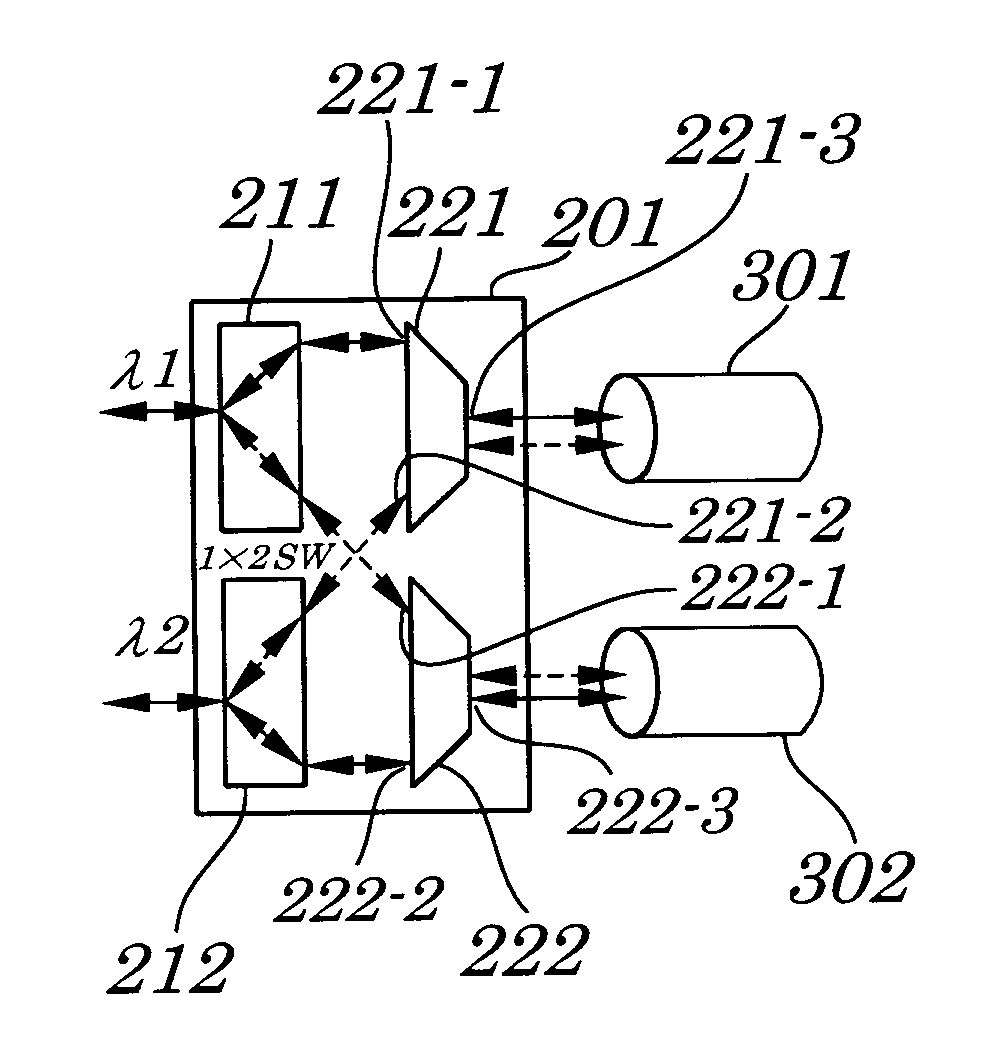
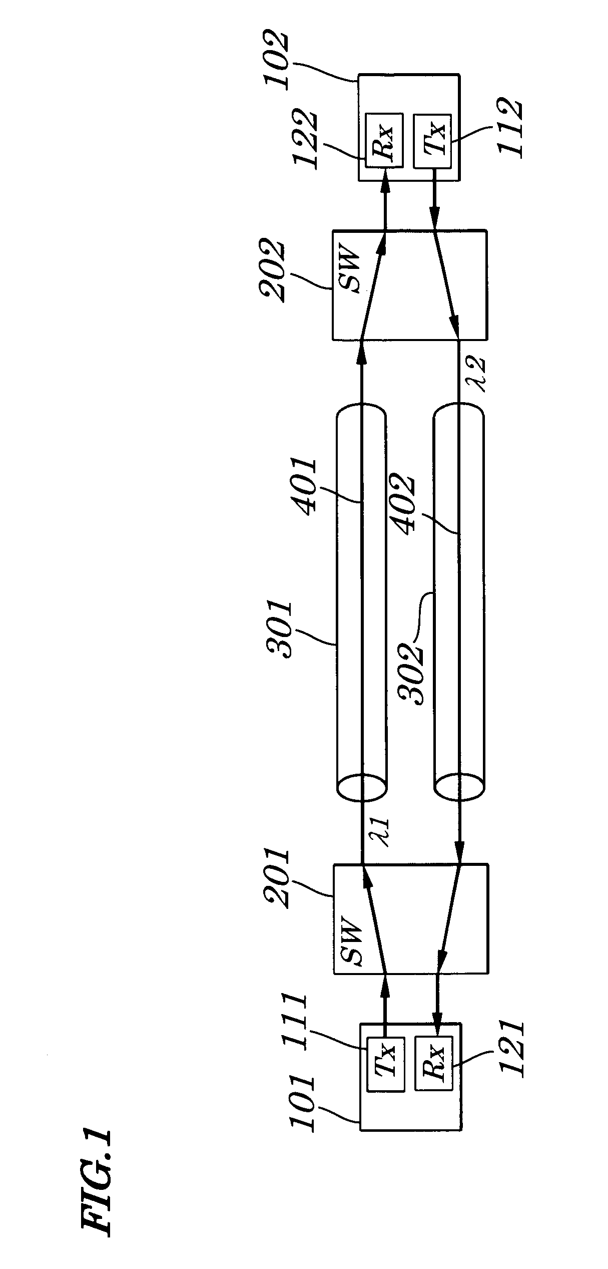
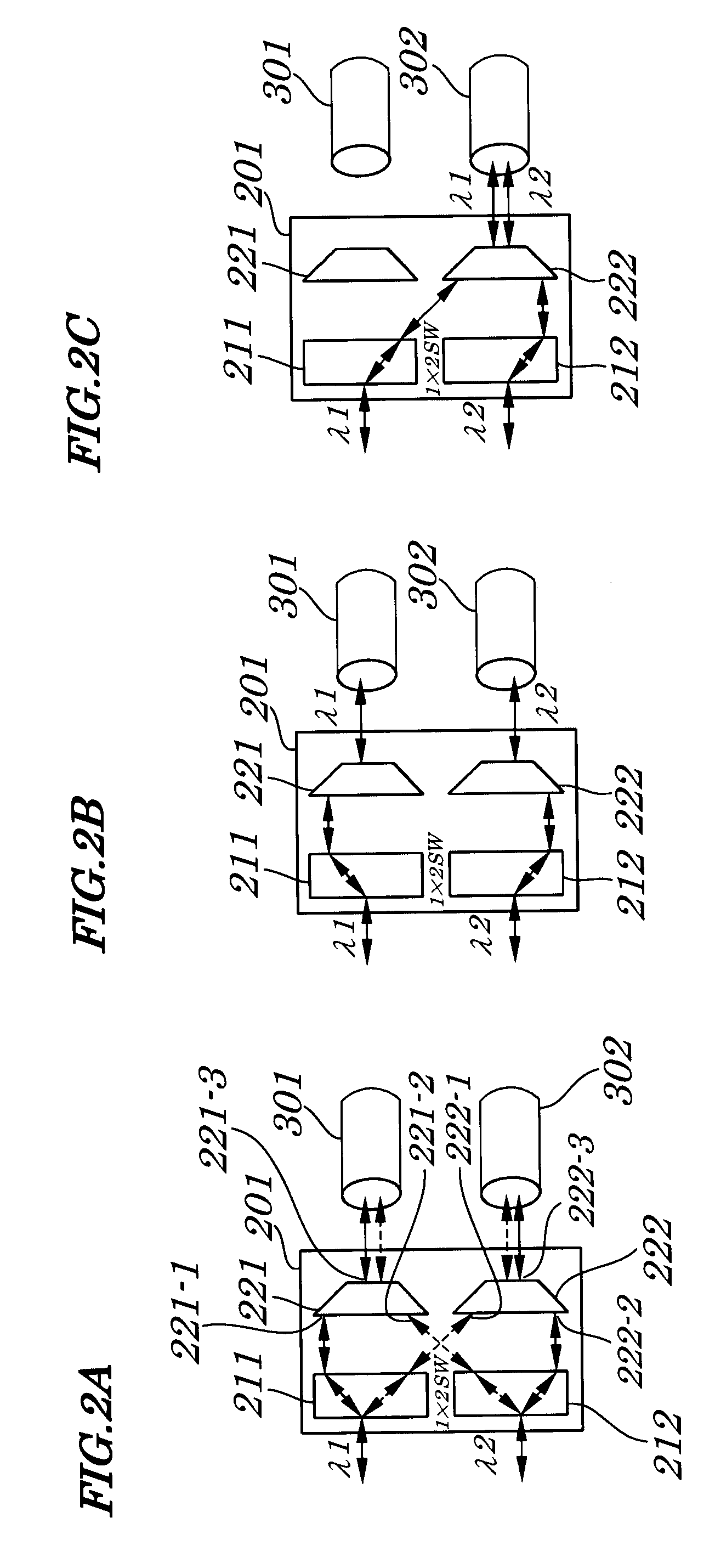
[0095]FIG. 1 is a block diagram showing configurations of an optical network system according to a first embodiment of the present invention. As shown in FIG. 1, the optical network system of the first embodiment is made up of optical signal transceivers 101 and 102, signal protection switches 201 and 202, and optical fiber transmission lines 301 and 302.

[0096]Each of the optical fiber transmission lines 301 and 302 is installed separately in a different path from each other. Therefore, there is almost no case where transmission failures of optical signals 401 and 402 occur in both of the optical fiber transmission lines 301 and 302 at a same time.

[0097]Each of the optical signal transceivers 101 and 102 has a same configuration and transmits and receives optical signals 401 and 402 in a direction opposite to each other. The optical signal transceiver 101 is made up of an optical signal transmitting section 111 and an optical signal receiving section 121. The optical signal transcei...

second embodiment

[0122]FIG. 5 is a block diagram showing configurations of an optical network system according to a second embodiment of the present invention. As shown in FIG. 5, the optical network system of the second embodiment is made up of optical signal transceivers 101, 102, 103, and 104, signal protection switches 601 and 602, and optical fiber transmission lines 301 and 302.

[0123]Each of the optical fiber transmission lines 301 and 302 is installed separately in a different path. Therefore, there is almost no case in which a failure occurs in both the optical fiber transmission lines 301 and 302 at a same time.

[0124]Configurations of the optical signal transceivers 101, 102, 103, and 104 are the same. The optical signal transceivers 101 and 102 are placed in a manner so as to face each other and transmit and receive optical signals to and from each other. Likewise, the optical signal transceivers 103 and 104 are placed in a manner so as to face each other and transmit and receive optical s...

third embodiment

[0159]FIG. 9 is a block diagram showing configurations of an optical network system according to a third embodiment of the present invention. As shown in FIG. 9, the optical network system of the third embodiment is a ring-type network having communication nodes 700-a, 700-b, 700-c, and 700-d and the optical fiber transmission lines 311, 312, 313, and 314.

[0160]The optical network system of the third embodiment has a function of having, if a failure occurs in any one of optical fiber transmission lines 311, 312, 313, or 314, an optical signal that had been transmitted through the optical fiber transmission line 311, 312, 313, or 314 in which the failure occurred begin to be transmitted in an optical fiber transmission line (311, 312, 313, or 314) placed in a ring in a reverse direction to bypass the optical fiber transmission line 311, 312, 313, or 314 in which the failure has occurred.

[0161]All the communication nodes 700-a, 700-b, 700-c, and 700-d have a same configuration and onl...


PUM


Abstract

An optical network system is provided which has a signal protection function and is able to be constructed of communication nodes manufactured at low costs. An optical signal transceiver has at least one optical signal transmitting device and at least one optical signal receiving device to transmit and receive an optical signal between nodes facing each other. A switching device, when no failure has occurred in the optical signal transmitting communication line and optical signal receiving communication line, transmits an optical signal from the optical signal transmitting device to an optical signal transmitting communication line and an optical signal having been received from the optical signal receiving communication line to an optical signal receiving device. The switching device, when a failure has occurred in the optical signal receiving communication line, does switching so as to be able to receive the optical signal, to be transmitted to the optical signal receiving device, from the optical signal transmitting communication line.

Description

BACKGROUND OF THE INVENTION[0001]1. Field of the Invention[0002]The present invention relates to a communication node and a switching device used in the communication node, and more particularly to the communication node making up a large-capacity and high-speed optical network and having a signal protection function for an optical signal communication line in the high-speed optical network, and the switching device used in the communication node.[0003]The present application claims priority of Japanese Patent Application No. 2002-209776 filed on Jul. 18, 2002, which is hereby incorporated by reference.[0004]2. Description of the Related Art[0005]Conventionally, in a large-capacity and high-speed optical network, a direction of a signal that can be transmitted by one piece of an optical fiber transmission line is only one direction.[0006]When bidirectional signals of an upward signal and a downward signal are to be transmitted between communication devices facing each other, two pie...

Claims


Application Information

Patent Timeline
IPC IPC(8): H04B10/00G02B6/35G02B6/42H04B10/03H04B10/032H04B10/038H04B10/07H04B10/25H04B10/27H04B10/275H04B10/278H04B10/291H04J14/00H04J14/02
CPCG02B6/3562H04J14/0289H04J14/0283G02B6/4246H04J14/0291
Inventor TAJIMA, AKIO
Owner NEC CORP
Why Eureka
Try Eureka