Mixer circuit

a mixer circuit and low frequency noise technology, applied in the field of mixer circuits, can solve the problems of flicker, large deterioration of the reception sensitivity of the entire system, above-described methods of improving the low frequency noise characteristics of the mixer circuit, etc., to reduce flicker noise, improve noise characteristics, and reduce frequency

Active Publication Date: 2009-11-03
PANASONIC SEMICON SOLUTIONS CO LTD
View PDF23 Cites 2 Cited by
  • Summary
  • Abstract
  • Description
  • Claims
  • Application Information

AI Technical Summary

Benefits of technology

[0062]According to the mixer circuit of claim 1, since the mixer circuit includes a mixer including an IF signal output load portion, an LO signal processing portion, and an RF signal processing portion, which are connected in cascade connection between a power supply and a ground; an RF signal supplier for supplying an RF signal to the RF signal processing portion; an LO signal supplier for supplying an LO signal to the LO signal processing portion; and at least a bypass current supply portion for bypassing a bias current of the LO signal processing portion, it is possible to reduce flicker noises occurring from the LO signal processing portion without reducing the gain of the mixer, thereby improving noise characteristics at lower frequency.
[0063]According to the mixer circuit of claim 2, since in the mixer circuit of claim 1, the bypass current supply portion is connected in parallel with the LO signal processing portion, it is possible to reduce the bias current of the LO signal processing portion without reducing the bias current of the RF signal processing portion, thereby reducing the NF.
[0064]According to the mixer circuit of claim 3, since in the mixer circuit of claim 1, the bypass current supply portion additionally supplies a bias current only to the RF signal processing portion, it is possible to reduce the bias current of the LO signal processing portion without reducing the bias current of the RF signal processing portion, thereby reducing the NF.
[0065]According to the mixer circuit of claim 4, since in the mixer circuit of claim 1, the bypass current supply portion includes a first bypass current source for additionally supplying a bias current only to the RF signal processing portion, and a second bypass current source for additionally supplying a bias current only to the IF signal output load portion, it is possible to reduce the bias current of the LO signal processing portion without reducing the bias current of the RF signal processing portion, thereby reducing the NF.
[0066]According to the mixer circuit of claim 5, since the mixer circuit includes a single balanced mixer including an IF signal output load portion, an LO signal processing portion, and an RF signal processing portion, which are connected in cascade connection between a supply voltage and a ground; an RF signal supplier for supplying an RF signal to the RF signal processing portion; an LO signal supplier for supplying an LO signal to the LO signal processing portion; at least one bypass current supply portion for bypassing a bias current of the LO signal processing portion; and said IF signal output load portion including a first load resistor having an end connected to the power supply and another end connected to a first IF output terminal, and a second load resistor having an end connected to the power supply and another end connected to a second IF output terminal; the RF signal processing portion including an RF transistor having a source terminal connected to the ground; said LO signal processing portion including a first LO transistor having a source terminal connected to a drain terminal of the RF transistor and a drain terminal connected to the first IF output terminal, and a second LO transistor having a source terminal connected to the drain terminal of the RF transistor and a drain terminal connected to the second IF output terminal, it is possible to reduce flicker noises occurring from the LO signal processing portion without reducing the gain of the mixer, thereby improving noise characteristics at lower frequencies.
[0067]According to the mixer circuit of claim 6, since in the mixer circuit of claim 5, since the bypass current supply portion includes a first bypass current source which is connected in parallel with the first LO transistor between the first IF output terminal and the drain terminal of the RF transistor, and a second bypass current source which is connected in parallel with the second LO transistor between the second IF output terminal and the drain terminal of the RF transistor, it is possible to reduce the bias current of the LO signal processing portion without reducing the bias current of the RF signal processing portion, thereby reducing NF.

Problems solved by technology

While the direct conversion system is an ideal receiving system as described above, it has following problems.
The problem is that since the frequency base band thereof is DC, it is likely to be affected by flicker noises with relative to the super heterodyne system.
Accordingly, in a receiver that employs a direct conversion system or a Low-IF system, the reception sensitivity of the entire system is greatly deteriorated due to the low-frequency noises of the mixer.
However, the above-described methods of improving the low frequency noise characteristics in the mixer circuit have following problems, respectively.
Therefore, it is not possible to take a so large value for the LW product.
Therefore, it is not possible to take a so large value for the W / L ratio.
Though the third conventional technique is effective to some extent when employing a high frequency device such as a bipolar that is superior in the low frequency noise characteristics, it is not so effective when employing MOS devices because the proportion of the flicker noises of the first and second LO transistors 21 and 22 are large.
Further, the sizes of the first and second load resistors 31 and 32 are required to be made quite large, and thereby there also arise problems in the circuit area, in the frequency characteristics of the IF signal, and the like.
As described above, the conventional mixer circuits do not have effective measures to reduce the low frequency noises, and particularly, it was not possible to obtain an improved reception sensitivity in a receiving system employing a direct conversion system or a Low-IF system.

Method used


Image

  • Mixer circuit
  • Mixer circuit
  • Mixer circuit

Examples


embodiment 1

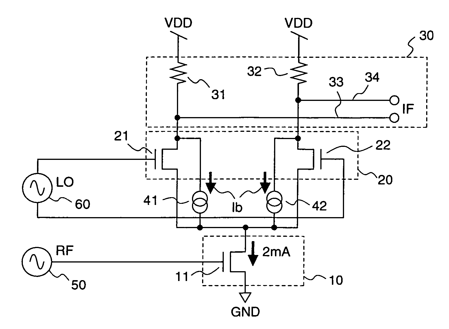
[0133]FIG. 1 is a circuit diagram illustrating a structure of a mixer circuit according to a first embodiment of the present invention.

[0134]As shown in FIG. 1, the mixer circuit according to the first embodiment has a basic structure of its mixer core part which is constituted by a single balanced mixer, and includes a single balanced mixer which is obtained by connecting an IF signal output load portion 30, an LO signal processing portion 20, and an RF signal processing portion 10 in cascade connection between a power supply VDD and a ground GND, an RF signal supplier 50 for supplying an RF signal to the RF signal processing portion 10, an LO signal supplier 60 for supplying LO signals to the LO signal processing portion 20, and first and second bypass current sources 41 and 42 which make bypass currents bypass the LO signal processing portion 20 with being connected in parallel with the LO signal processing portion 20.

[0135]The IF signal output load portion 30 includes a first lo...

embodiment 2

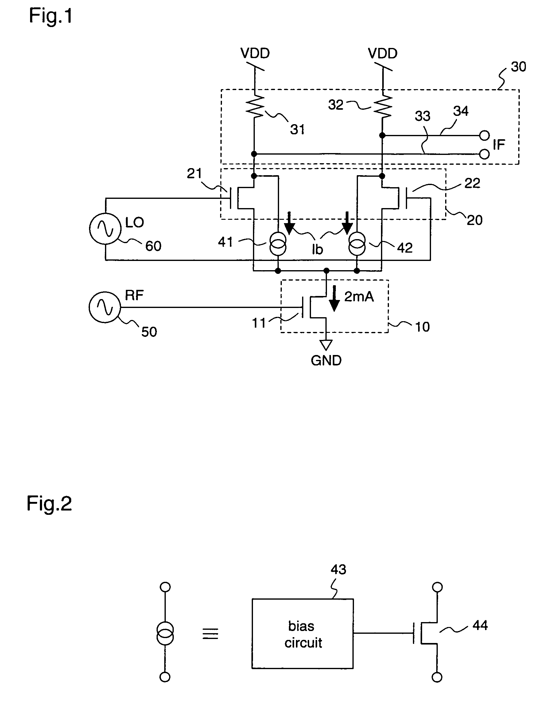
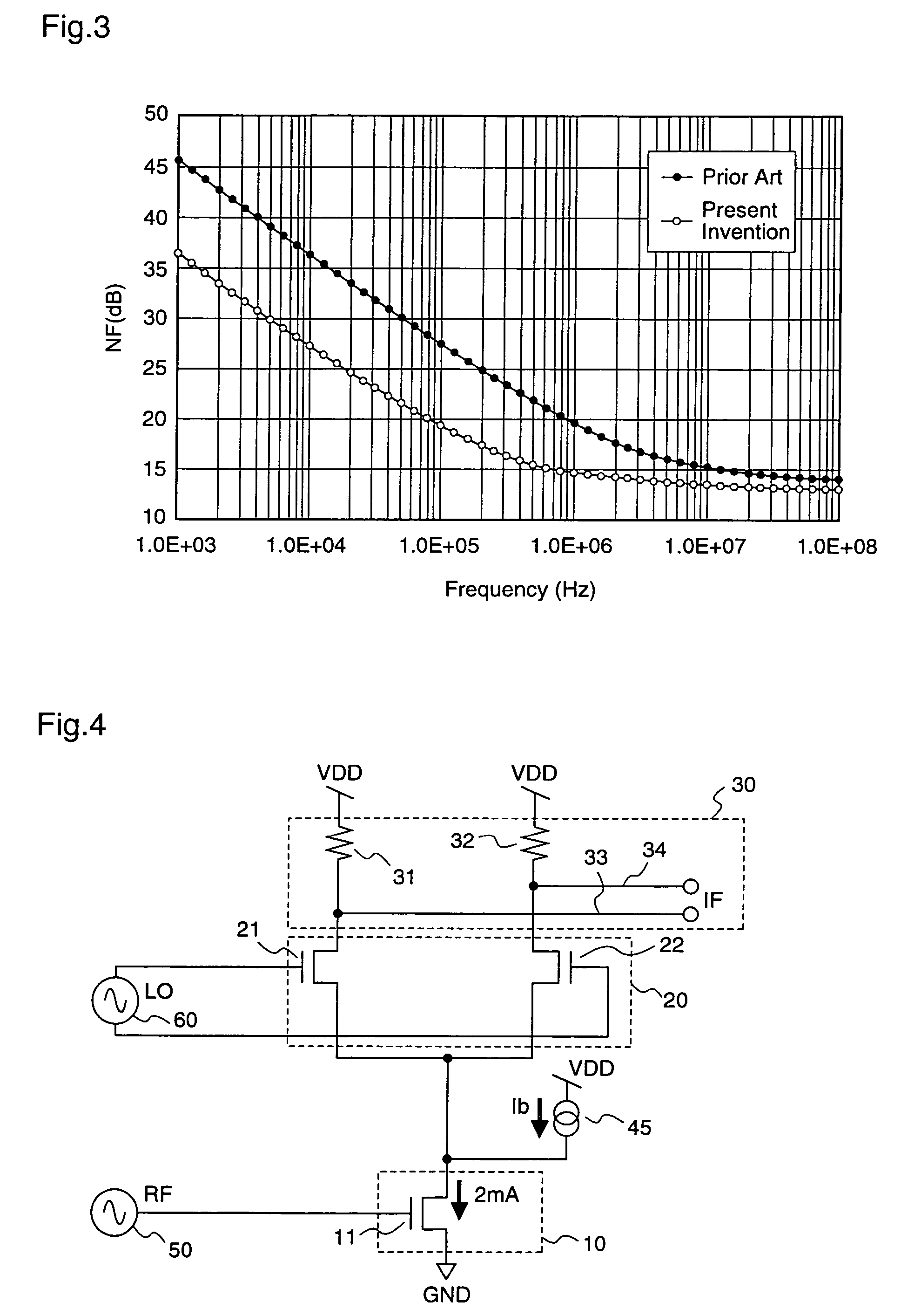
[0151]FIG. 4 is a circuit diagram illustrating a construction of a mixer circuit according to a second embodiment of the present invention. In FIG. 4, the same or corresponding parts as in FIG. 1 are denoted by the same reference numerals, and their detailed descriptions are omitted.

[0152]As shown in FIG. 4, in the mixer circuit according to the second embodiment, a first bypass current source 45 is connected between the power supply VDD and the drain terminal of the RF transistor 11, so as to additionally supply a bias current only to the RF transistor 11. The first bypass current source 45 is covered by a bypass current supply portion described in claim 7.

[0153]The first bypass current source 45 may be, for example, one which includes the bias circuit 43 and the current source transistor 44, as shown in FIG. 2. Further, it may generate bypass currents by any elements or circuits which realize constant current source characteristics.

[0154]The operation of the mixer circuit accordin...

embodiment 3

[0165]FIG. 6 is a circuit diagram illustrating a structure of a mixer circuit according to a third embodiment of the present invention. In FIG. 6, the same or corresponding parts as in FIG. 4 are denoted by the same reference numerals, and their detailed descriptions are omitted.

[0166]As shown in FIG. 6, the mixer circuit according to the third embodiment includes, in addition to that the mixer circuit of the second embodiment of the present invention is provided with the first bypass current source 45 that additionally supplies the bias current only to the RF transistor 11, further a second bypass current source 46 that is connected between the first IF output terminal 33 and the ground GND thereby to additionally supply a bias current only to the first load resistor 31, and a third bypass current source 47 that is connected between the second IF output terminal 34 and the ground GND thereby to additionally supply a bias current only to the second load resistor 32. The first to thi...


PUM


Abstract

A mixer circuit of a receiving system, requiring low noise characteristics at lower frequency, includes a bypass current source (41) which is connected in parallel with an LO transistor (21) between an IF output terminal (33) and a drain terminal of an RF transistor (11), and a bypass current source (42) which is connected in parallel with an LO transistor (22) between an IF output terminal (34) and the drain terminal of the RF transistor (11), thereby decreasing a current flowing through the LO transistors (21, 22) without decreasing a bias current flowing through the RF transistor (11). Accordingly, it is possible to suppress flicker noises occurring from the LO transistors (21, 22) without lowering the gain of the mixer, thereby realizing a mixer circuit with excellent low frequency noise characteristics, which can improve the NF characteristics at lower frequency.

Description

RELATED APPLICATION[0001]This application is a national phase of PCT / JP2004 / 016938 filed on Nov. 15, 2004, which claims priority from Japanese Application No. 2003-400262 filed on Nov. 28, 2003, the disclosures of which Applications are incorporated by reference herein. The benefit of the filing and priority dates of the International and Japanese Applications is respectfully requested.TECHNICAL FIELD[0002]The present invention relates to a mixer circuit in a receiving system, in particular, in a radio communication apparatus employing such as a direct conversion system or a Low-IF system in which low noise characteristics at low frequencies is required.BACKGROUND ART[0003]As a receiving system in a radio communication apparatus, there are a super-heterodyne system, a direct conversion system, a Low-IF system, or the like. While the receiving system which is most dominant at present is the super-heterodyne system, the direct conversion system and the Low-IF system have been recently...

Claims


Application Information

Patent Timeline
Patent Type & Authority Patents(United States)
IPC IPC(8): H04B1/18H04B1/26H03D7/00H03D7/14
CPCH03D7/1441H03D7/1433H03D7/1458H03D2200/0084H03D2200/0043
Inventor HIJIKATA, KATSUMASAHAYASHI, JOJI
Owner PANASONIC SEMICON SOLUTIONS CO LTD
Why Eureka
Try Eureka