Formation of silicon nitride film

a technology of silicon nitride and film, applied in the direction of crystal growth process, polycrystalline material growth, chemically reactive gases, etc., can solve the problem of low film stress inability to achieve the desired stress strength, and small selectivity of silicon nitride film over an oxide film etching rate, etc. problem, to achieve the effect of low wet-etch ra

Active Publication Date: 2009-12-01
TOKYO ELECTRON LTD
View PDF24 Cites 54 Cited by
  • Summary
  • Abstract
  • Description
  • Claims
  • Application Information

AI Technical Summary

Benefits of technology

[0006]The present invention has been made in view of the aforementioned problems, and it is therefore an object of the present invention to provide a technique for forming a silicon nitride film having a high stress at a low process temperature.
[0007]Another object of the present invention is to provide a technique for forming a silicon nitride film having a low wet-etch rate.
[0008]Another object of the present invention is to provide a technique for controlling a stress of a silicon nitride film.

Problems solved by technology

However, a silicon nitride film deposited at a low process temperature by using an ALD process has a high wet-etch rate, and thus, the etching selectivity of the silicon nitride film over an oxide film is small.
Moreover, a silicon nitride film deposited under a low process temperature has a low film stress, and cannot achieve desired stress strength.

Method used


Image

  • Formation of silicon nitride film
  • Formation of silicon nitride film
  • Formation of silicon nitride film

Examples


Embodiment Construction

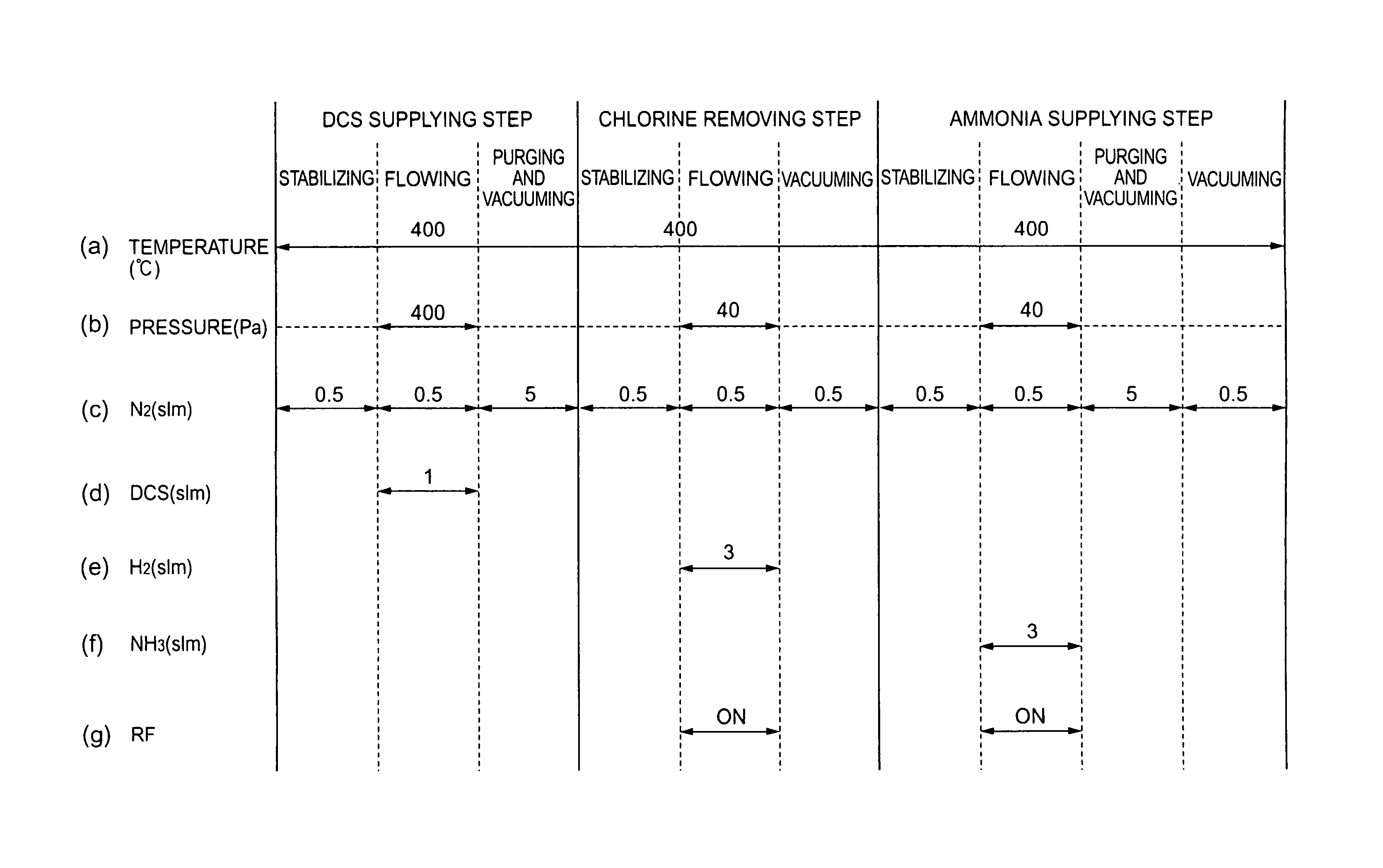
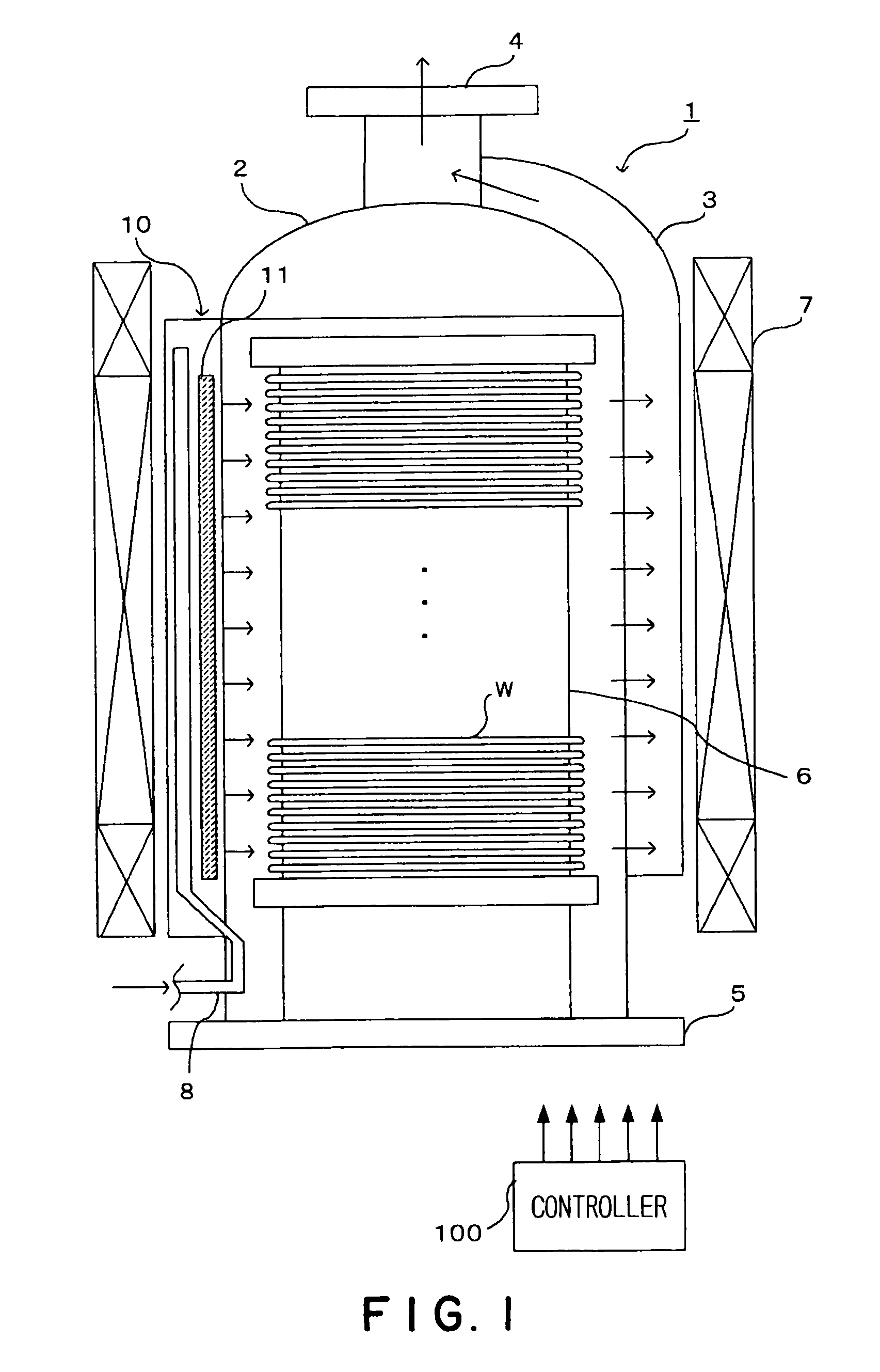
[0023]A preferred embodiment of the present invention will be described with reference to the attached drawings. In the illustrated embodiment described below, a batch-type, vertical processing apparatus is used as an apparatus for forming a silicon nitride film.

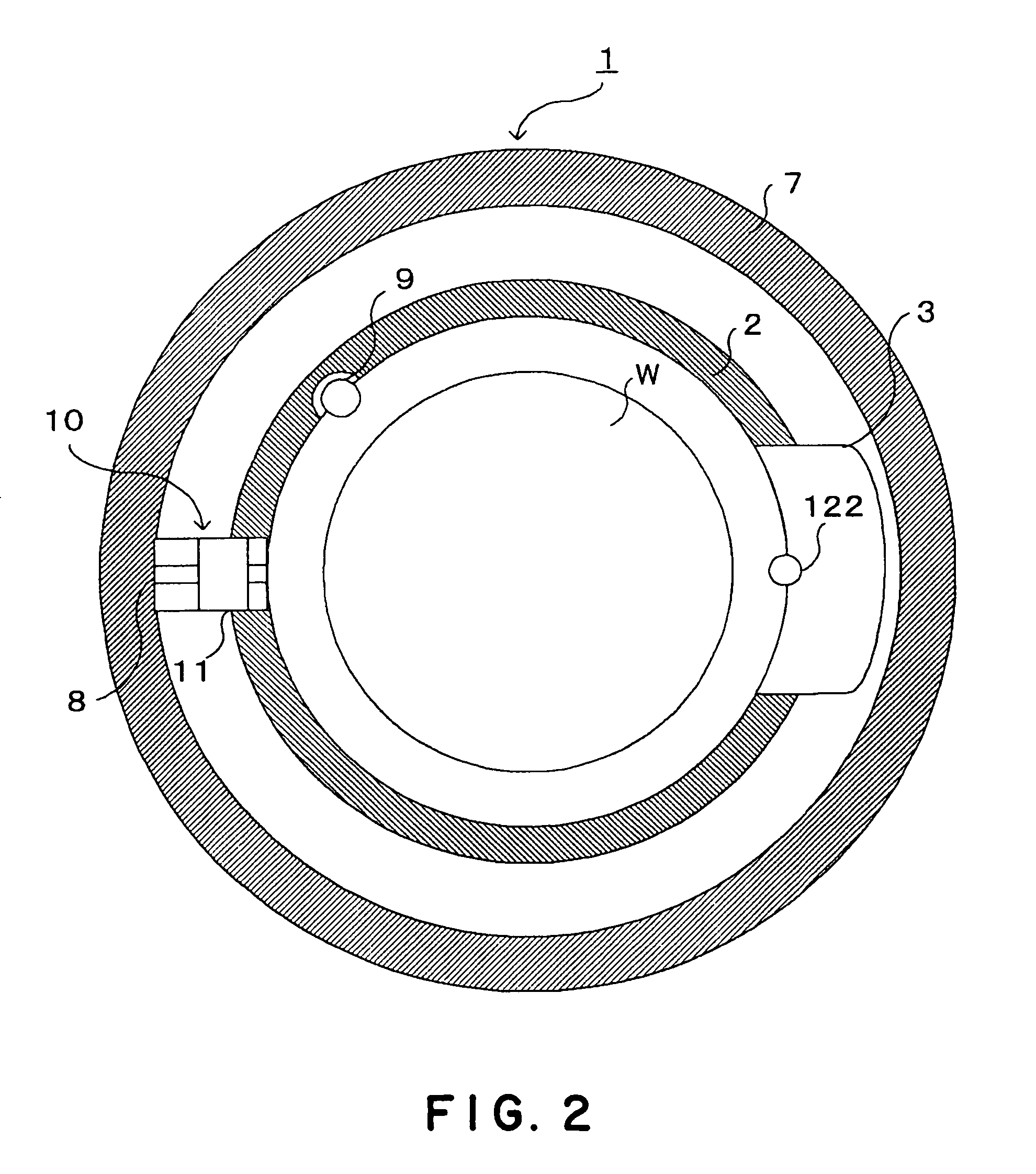
[0024]As shown in FIG. 1, a processing apparatus 1 includes a reaction tube having a cylindrical shape with its longitudinal axis being directed to a vertical direction. The reaction tube 2 is made of a heat-resistant, corrosion-resistant material such as quartz.

[0025]An exhaust chamber 3 is arranged on one side of the reaction tube 2 to discharge gases in the reaction tube 2. The exhaust chamber 3 is connected to an interior of the reaction tube 2 through an opening, which is formed in a side wall of the reaction tube 2 and extends vertically. The top end of the exhaust chamber 3 is connected to an exhaust port 4 arranged at the top of the reaction tube 2. Connected to the exhaust port 4 is a not shown exhaust pipe, in whic...


PUM

PropertyMeasurementUnit
pressureaaaaaaaaaa
internal pressureaaaaaaaaaa

Abstract

A method of forming a silicon nitride film which can form a silicon nitride film having a high film stress at a low process temperature is described herein. The method includes the steps of (a) supplying dichlorosilane into a reaction chamber containing a process object, thereby allowing chemical species originated from dichlorosilane as a precursor to be adsorbed on the process object; (b) hydrogenating chlorine contained in the chemical species, thereby removing the chlorine from the chemical species; and (c) supplying ammonia radicals into the reaction chamber, thereby nitriding the chemical species, from which the chlorine has been removed, by the ammonia radicals to, deposit resultant silicon nitride on the process object, wherein the steps (a), (b) and (c) are performed repeatedly for plural times in that order, thereby a silicon nitride film of a desired thickness is formed on a semiconductor wafer.

Description

TECHNICAL FIELD[0001]The present invention relates to a technique for forming a silicon nitride film.BACKGROUND ART[0002]A semiconductor device fabricating process includes a step of forming a silicon nitride film on a process object such as a semiconductor wafer by using an ALD process.[0003]The ALD process alternately supplies two (or more) different source gases one by one onto a process object under predetermined process conditions, so that chemical species is adsorbed to the process object at a single atomic layer level, and are deposited on the process object through surface reactions. For instance, first and second source gases are alternately supplied to a process object to flow along the surface thereof, thereby molecules contained in the first source gas adsorb to the surface, and molecules contained in the second source gas react with the adsorbed molecules originated from the first source gas to form a film of a thickness of a single molecule level. The above process ste...

Claims


Application Information

Patent Timeline
Patent Type & Authority Patents(United States)
IPC IPC(8): H05H1/24
CPCC23C16/345C23C16/45546C23C16/45542H01L21/0228H01L21/02274C23C16/45553H01L21/0217H01L21/02211
Inventor MATSUURA, HIROYUKI
Owner TOKYO ELECTRON LTD
Why Eureka
Try Eureka