Data inversion register technique for integrated circuit memory testing

a data inversion register and integrated circuit technology, applied in the direction of error prevention, digital transmission, instruments, etc., can solve the problems of inability to write data stripes from a single data input signal, lack of pattern capability needed to exercise the full memory array and data path, and difficulty in manufacturing testing of these wide i/o dram circuits. to achieve the effect of maximizing the probability of identifying failures

Active Publication Date: 2009-12-08
INVENSAS CORP
View PDF4 Cites 19 Cited by
  • Summary
  • Abstract
  • Description
  • Claims
  • Application Information

AI Technical Summary

Benefits of technology

[0004]The data inversion register technique of the present invention is, therefore, operative to invert data input signals in a predetermined pattern to maximize the probability of identifying failures and defects during testing of memory arrays.
[0007]The technique of the present invention therefore allows for a reduced number of data inputs (all the way down to and including one) to be supplied to the DRAM. For example, for ease of testing, one data bit can be supplied to all of the DRAM chip or macro block data inputs. In accordance with the present invention, a more interesting data pattern can be applied to the actual memory array than simply all “ones” or “zeroes”.
[0008]The data outputs may also be multiplexed, or compressed down, to a reduced number, all the way down to and including a single output if desired. In accordance with one embodiment of the present invention disclosed herein, the output data path is simply matched to the data in path with an ID controlled inverter. Another embodiment of the present invention contemplates multiplexing the data down to a more narrow output width for testing ease and control which data bits get inverted with the actual multiplexed addresses. This serves to reduce the number of data inverters needed on the output path.

Problems solved by technology

Manufacturing testing of these wide I / O DRAM circuits is particularly challenging.
Data compression test modes have been used to meet this challenge but these techniques lack the pattern capability needed to exercise the full memory array and data path.
Further, conventional data path circuits do not have the capability for writing data stripes from a single data input signal.

Method used


Image

  • Data inversion register technique for integrated circuit memory testing
  • Data inversion register technique for integrated circuit memory testing
  • Data inversion register technique for integrated circuit memory testing

Examples


Embodiment Construction

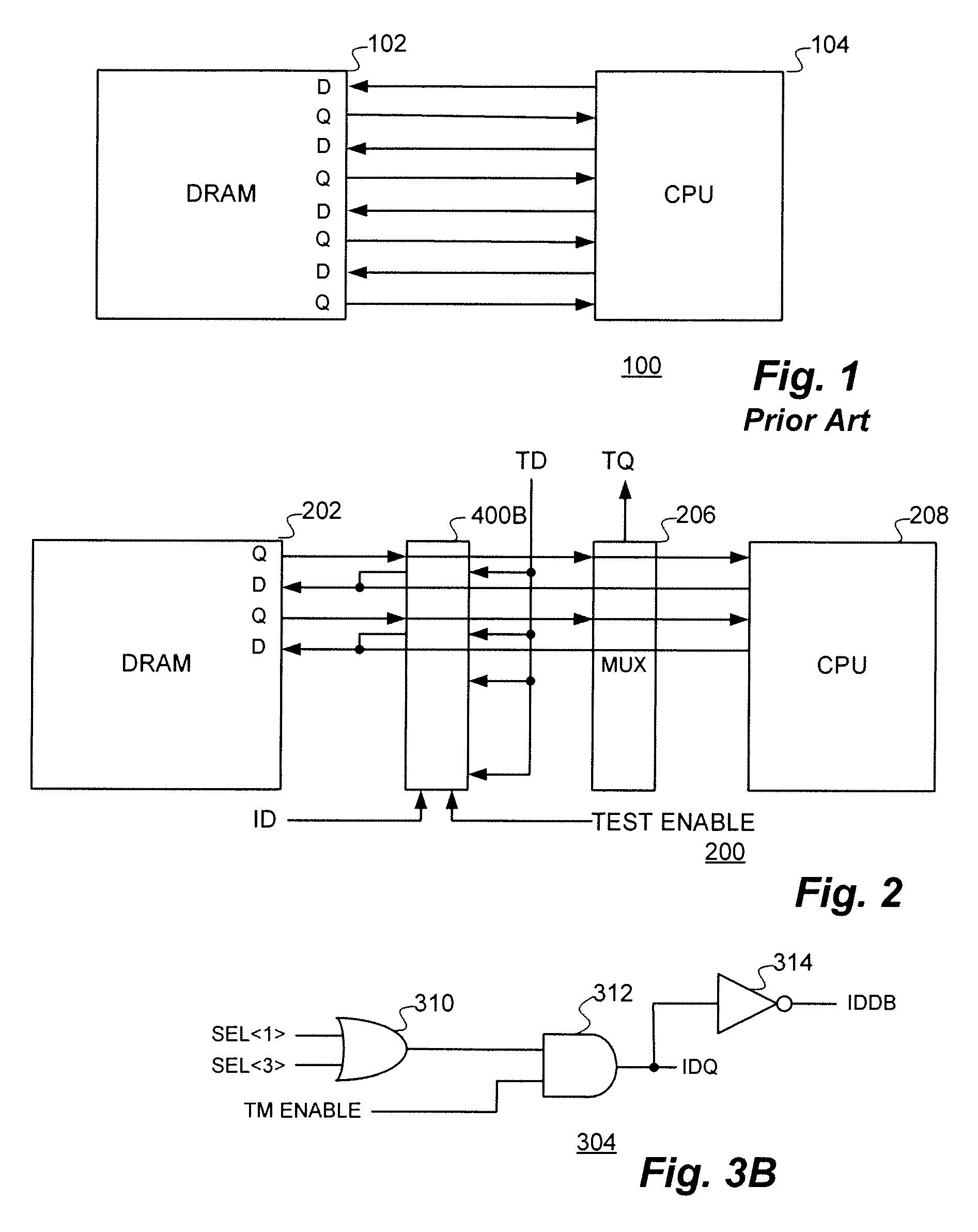
[0020]With reference now to FIG. 1, a simplified functional block diagram illustrative of a prior art circuit 100 interconnection of a DRAM 102 with a central processing unit (CPU) 104 by means of a number of data input (D) and data output (Q) lines is shown.

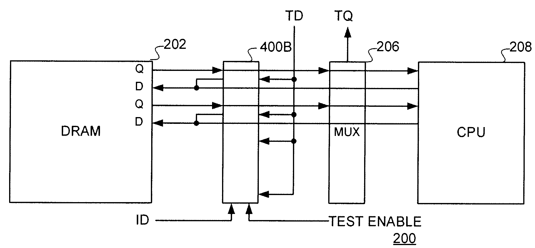
[0021]With reference additionally now to FIG. 2, a corresponding simplified functional block diagram of a representative testing configuration 200 is shown for implementing the data inversion register technique of the present invention. In this illustration, a number of test mode input drivers 400B and a multiplexer 206 are coupled between a DRAM 202 and a CPU 208. The test mode input drivers 400B receive an invert data (ID) signal and TEST ENABLE signal in addition to input test data (TD). As shown, the multiplexer 206 ultimately outputs the test data (TQ).

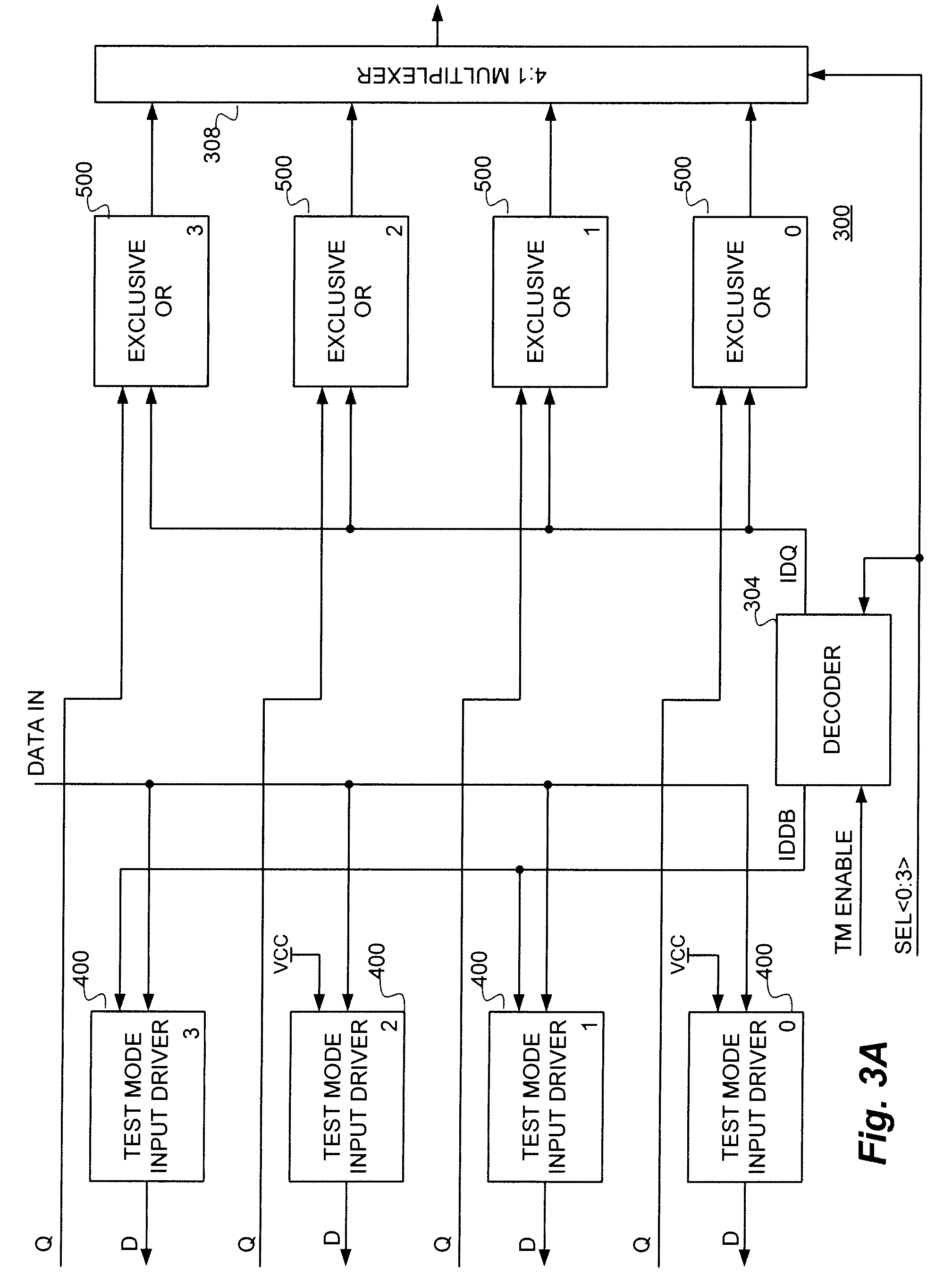
[0022]With reference additionally now to FIG. 3A, another simplified functional block diagram of a further representative testing configuration 300 is shown for implementing ...


PUM


Abstract

A data inversion register technique for integrated circuit memory testing in which data input signals are selectively inverted in a predetermined pattern to maximize the probability of identifying failures during testing. In accordance with the technique of the present invention, on predetermined input / outputs (I / Os,) data inputs may be inverted to create a desired test pattern (such as data stripes) which are “worst case” for I / O circuitry or column stripes which are “worst case” for memory arrays. A circuit in accordance with the technique of the present invention then matches the pattern for the data out path, inverting the appropriate data outputs to obtain the expected tester data. In this way, the test mode is transparent to any memory tester.

Description

BACKGROUND OF THE INVENTION[0001]The present invention relates, in general, to the field of integrated circuit memory devices and those devices incorporating embedded memory. More particularly, the present invention relates to a data inversion register technique for integrated circuit memory testing which results in a maximization of the probability of identifying device failures during testing.[0002]With today's standard dynamic random access memory (DRAM) devices, input / output (I / O) widths are becoming ever larger with 32 bit widths and wider being relatively common. In comparison, embedded DRAM circuits may contain even wider I / O widths including those having 256 data in (Din) and 256 data out (Dout) widths and wider.[0003]Manufacturing testing of these wide I / O DRAM circuits is particularly challenging. Data compression test modes have been used to meet this challenge but these techniques lack the pattern capability needed to exercise the full memory array and data path. Further...

Claims


Application Information

Patent Timeline
Patent Type & Authority Patents(United States)
IPC IPC(8): G11C29/00H04L1/00
CPCG01R31/31713G11C29/56G11C29/10G11C2029/0409
Inventor PARRIS, MICHAEL C.JONES, JR., OSCAR FREDERICK
Owner INVENSAS CORP
Why Eureka
Try Eureka