Wafer level package utilizing laser-activated dielectric material

a laser-activated dielectric and wafer-level technology, applied in the direction of semiconductor devices, semiconductor/solid-state device details, electrical equipment, etc., can solve the problems of high associated cost and inherently slow multi-step process, and achieve the effect of low cos

Active Publication Date: 2009-12-15
AMKOR TECH SINGAPORE HLDG PTE LTD
View PDF14 Cites 57 Cited by
  • Summary
  • Abstract
  • Description
  • Claims
  • Application Information

AI Technical Summary

Benefits of technology

[0008]In the above manner, the embedded circuit pattern is fo

Problems solved by technology

Although effective in producing a circuit pattern, the multi-ste

Method used


Image

  • Wafer level package utilizing laser-activated dielectric material
  • Wafer level package utilizing laser-activated dielectric material
  • Wafer level package utilizing laser-activated dielectric material

Examples


Embodiment Construction

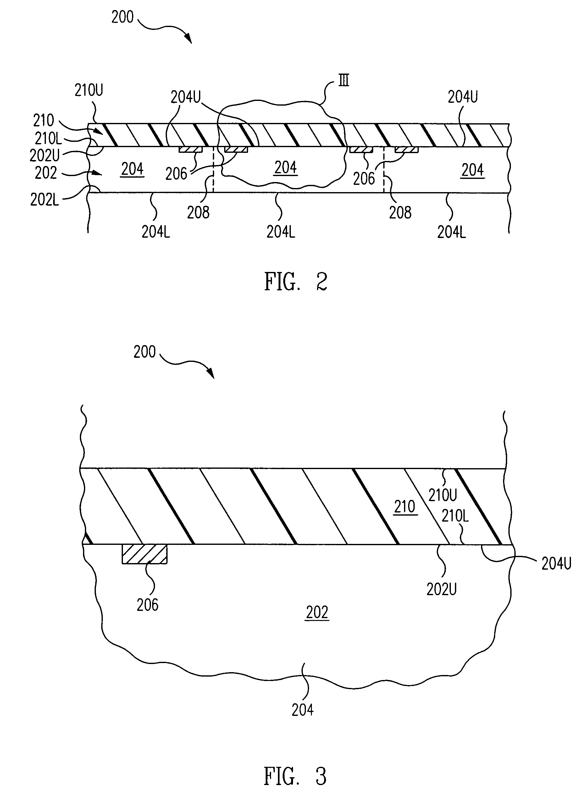
[0019]In accordance with one embodiment, referring to FIGS. 1, 2 and 3 together, a method 100 of forming a wafer level package includes attaching a laser-activated dielectric material 210 to an integrated circuit substrate 202 to form an assembly 200 (operation 104). Integrated circuit substrate 202 including a plurality of electronic components 204 having terminals 206 on first surfaces 204U thereof.

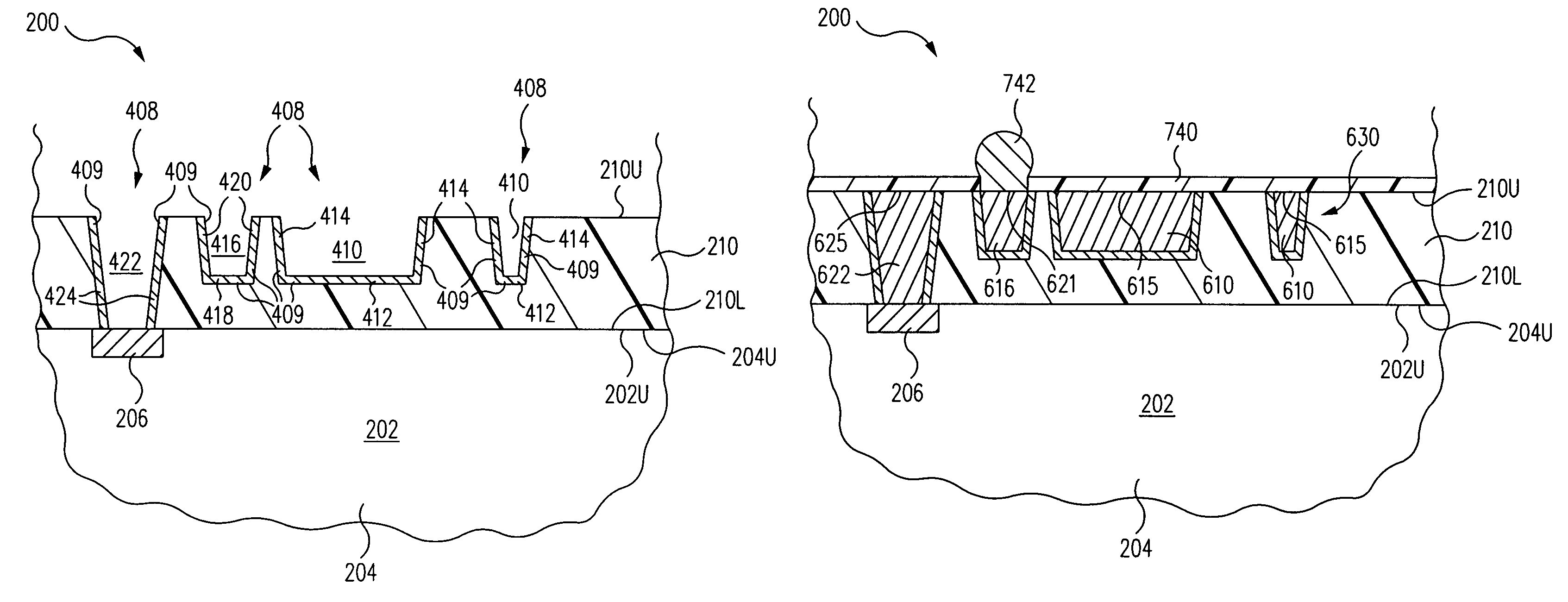
[0020]Referring now to FIGS. 1, 4 and 5 together, laser-activated dielectric material 210 is laser activated and ablated with a laser (operation 106) to form laser-ablated artifacts 408 in laser-activated dielectric material 210 and simultaneously to form an electrically conductive laser-activated layer 409 lining laser-ablated artifacts 408.

[0021]Referring now to FIGS. 1, 5 and 6 together, laser-ablated artifacts 408 are filled using an electroless plating process in which an electrically conductive filler material 628 is selectively plated on laser-activated layer 409 to form an embed...


PUM


Abstract

A method of forming a wafer level package includes attaching a laser-activated dielectric material to an integrated circuit substrate to form an assembly, the integrated circuit substrate including a plurality of electronic components having terminals on first surfaces thereof. The laser-activated dielectric material is laser activated and ablated with a laser to form laser-ablated artifacts in the laser-activated dielectric material and simultaneously to form an electrically conductive laser-activated layer lining the laser-ablated artifacts. The laser-ablated artifacts are filled using an electroless plating process in which an electrically conductive filler material is selectively plated on the laser-activated layer to form an embedded circuit pattern within the laser-activated dielectric material.

Description

BACKGROUND OF THE INVENTION[0001]1. Field of the Invention[0002]The present invention relates generally to packaging of electronic components. More particularly, the present invention relates to a method of fabricating a wafer level package and the resulting structure.[0003]2. Description of the Related Art[0004]To form a circuit pattern, features in a dielectric layer are filled with plated copper. Typically, this entails formation of the features in the dielectric layer, formation of an electrically conductive seed layer within the features, and filling of the features by plating copper on the electrically conductive seed layer within the features.[0005]Although effective in producing a circuit pattern, the multi-step process is inherently slow and thus has a high associated cost.SUMMARY OF THE INVENTION[0006]In accordance with one embodiment, a method of forming a wafer level package includes attaching a laser-activated dielectric material to an integrated circuit substrate to fo...

Claims


Application Information

Patent Timeline
IPC IPC(8): H01L21/4763H01L21/44H01L23/04H01L23/48H01L23/52H01L23/538H01L29/40
CPCH01L21/76804H01L21/76843H01L21/76874H01L23/5329H01L23/525H01L23/5328H01L21/76879H01L2224/05001H01L2224/05026H01L2224/11H01L2224/13025H01L2924/00014H01L2924/0002H01L2924/12044H01L2924/00H01L2224/05599H01L2224/05099
Inventor RUSLI, SUKIANTOKUO, BOB SHIH-WEIHUEMOELLER, RONALD PATRICK
Owner AMKOR TECH SINGAPORE HLDG PTE LTD
Why Eureka
Try Eureka