Apparatus, system, and method for joint processing in graphics processing units

Active Publication Date: 2009-12-15
NVIDIA CORP
View PDF18 Cites 44 Cited by
  • Summary
  • Abstract
  • Description
  • Claims
  • Application Information

AI Technical Summary

Problems solved by technology

However, increasing the number of parallel processing elements in stage n has the drawback that the chip area devoted to stage n increases.
A larger chip size, in turn, increases the cost to produce GPU chip 100.
As a result, the cost of a GPU chip also increases if the production volume decreases below some minimum level.
It is difficult for GPU manufacturers to design a chip that achieves a satisfactory tradeoff of cost and performance for a broad cross-section of consumers.
However, a large portion of the market is cost sensitive and does not require the highest level of performance.
Conventionally, GPU manufacturers have difficulty simultaneously serving the different market segments.
A GPU chip designed only for the market segment demanding the highest performance would be too expensive for price-sensitive consumers and may also have a production run that has too small a volume to take full advantage of economies of scale.
Conversely, a GPU chip designed for price-sensitive consumers will not have the performance desired by high-end consumers.

Method used


Image

  • Apparatus, system, and method for joint processing in graphics processing units
  • Apparatus, system, and method for joint processing in graphics processing units
  • Apparatus, system, and method for joint processing in graphics processing units

Examples


Embodiment Construction

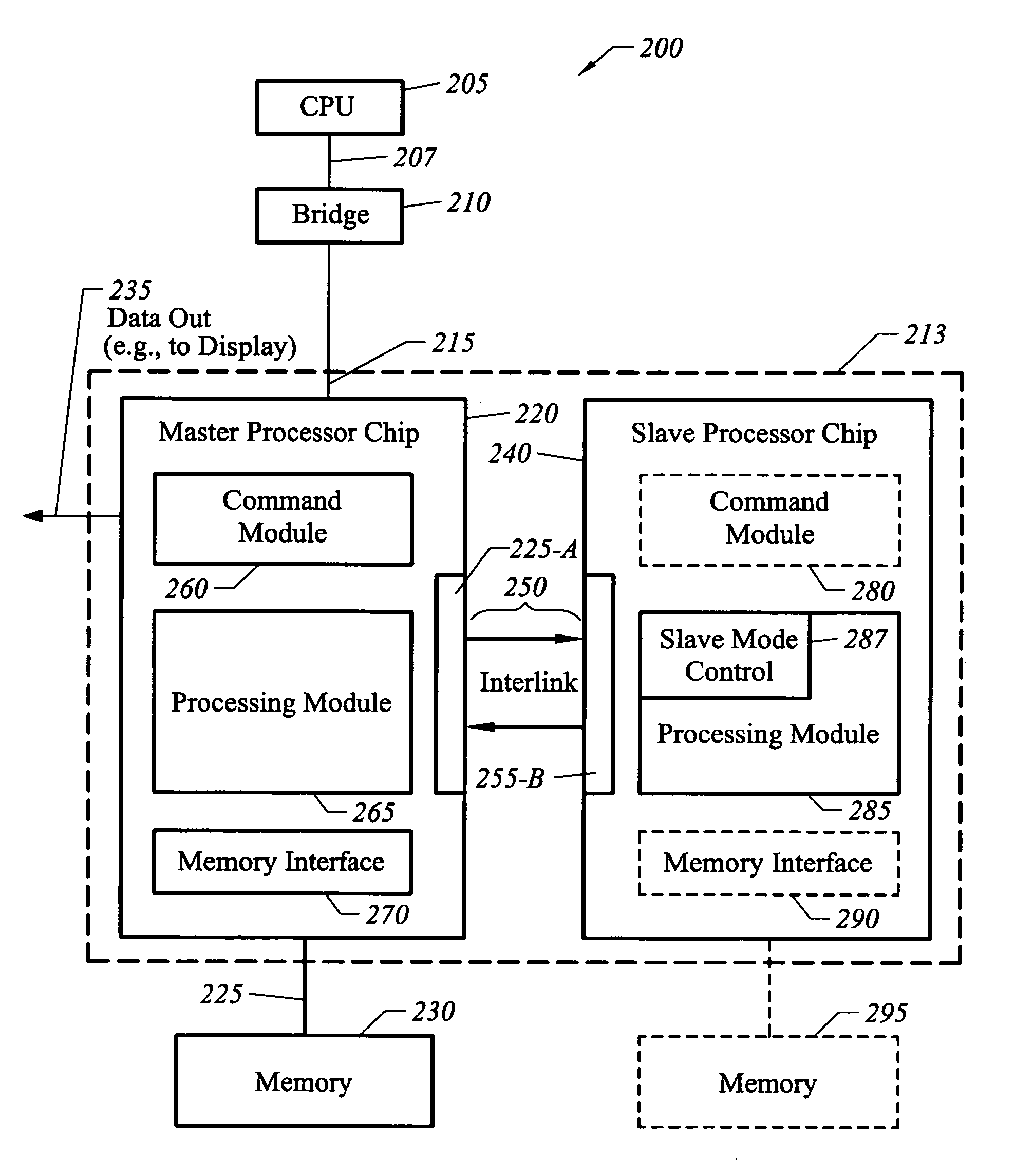
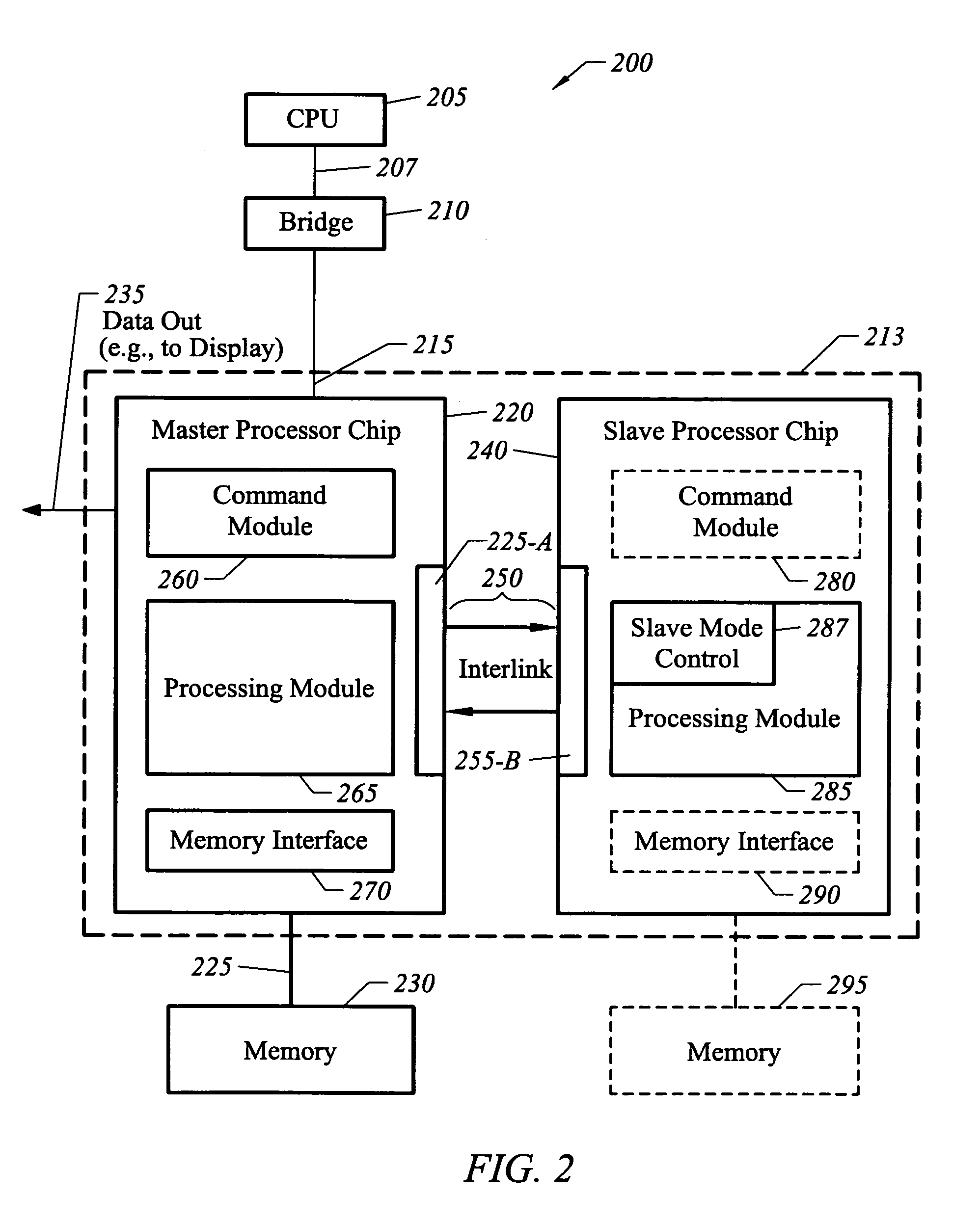
[0024]FIG. 2 is a block diagram of a multi-chip graphics system 200 in accordance with one embodiment of the present invention. A central processing unit (GPU) 205 is coupled to a graphics processing unit (GPU) chip 220 through a suitable bus interface. As used in this application a “chip” is an integrated circuit that resides on a die, with the die packaged to permit electrical power and signal connections to be made to the integrated circuit.

[0025]In one embodiment, a bridge 210, such as a bridge chipset, is used to couple GPU 205 to GPU chip 220. For example, a front side bus 207 may be used to communicatively couple GPU 205 to bridge 210 whereas a performance component interface (PCI)-Express bus 215 may be used to communicatively couple GPU chip 220 to bridge 210. PCI-Express is a high speed interface standard promoted by the PCI-SIG organization and defined by the PCI-Express specification published by PCI-SIG, the contents of which are hereby incorporated by reference. A grap...


PUM


Abstract

A multi-chip graphics system includes a master chip and a slave chip coupled by an interlink. The slave chip performs pixel processing in parallel with the master chip, improving the performance of the master chip. In one embodiment, an individual graphics processing unit (GPU) chip includes a normal operational mode, a master mode, and a slave mode to permit an individual GPU chip to be used as individual processor or to be utilized as part of a master / slave pair.

Description

RELATED APPLICATIONS[0001]This application is related to the commonly owned patent application entitled “Multi-chip Graphics Processing Unit Apparatus, System, and Method” Application Ser. No. 10 / 992,276, the contents of which are hereby incorporated by reference.FIELD OF THE INVENTION[0002]The present invention is generally related to improving the performance of a graphics processing unit. More particularly, the present invention is directed to a graphics processing unit chip that may be used as an individual processor or utilized with another graphics processing unit chip to improve performance.BACKGROUND OF THE INVENTION[0003]The design of a graphics processing unit (GPU) chip includes many different tradeoffs. FIG. 1 is a block diagram of a prior art GPU chip 100. A GPU is typically implemented as a sequence of pipelined stages, where each stage is dedicated to performing a particular graphics processing operation. Some stages, such as stage n, can be implemented by two or more...

Claims


Application Information

Patent Timeline
IPC IPC(8): G06F15/16G06F13/14G06F15/80
CPCG06T1/20
Inventor KELLEHER, BRIAN M.
Owner NVIDIA CORP
Why Eureka
Try Eureka