Current protection circuit using multiple sequenced bipolar transistors

a current protection circuit and bipolar transistor technology, applied in the direction of transistors, electrical devices, arrangements responsive to excess voltage, etc., can solve the problem of unidirectional current protection circuits, and achieve the effect of reducing the current triggering voltage differential and effective triggering of current protection

Inactive Publication Date: 2009-12-22
SEMICON COMPONENTS IND LLC
View PDF11 Cites 2 Cited by
  • Summary
  • Abstract
  • Description
  • Claims
  • Application Information

AI Technical Summary

Benefits of technology

[0007]As compared to using a single bipolar transistor, the use of such sequenced bipolar transistors reduces the current triggering voltage differential between the protected circuit node and the current source or sink. This allows for effective triggering of current protection for a protected circuit node without requiring a zener diode. This may also permit the area of the current protection circuit to be smaller since even a sequence of bipolar transistors may be smaller than a zener diode with similar current-voltage characteristics. Furthermore, the current protection circuit may be made to be unidirectional, whereas a zener diode on its own is bidirectional.

Problems solved by technology

Furthermore, the current protection circuit may be made to be unidirectional, whereas a zener diode on its own is bidirectional.

Method used


Image

  • Current protection circuit using multiple sequenced bipolar transistors
  • Current protection circuit using multiple sequenced bipolar transistors
  • Current protection circuit using multiple sequenced bipolar transistors

Examples


Embodiment Construction

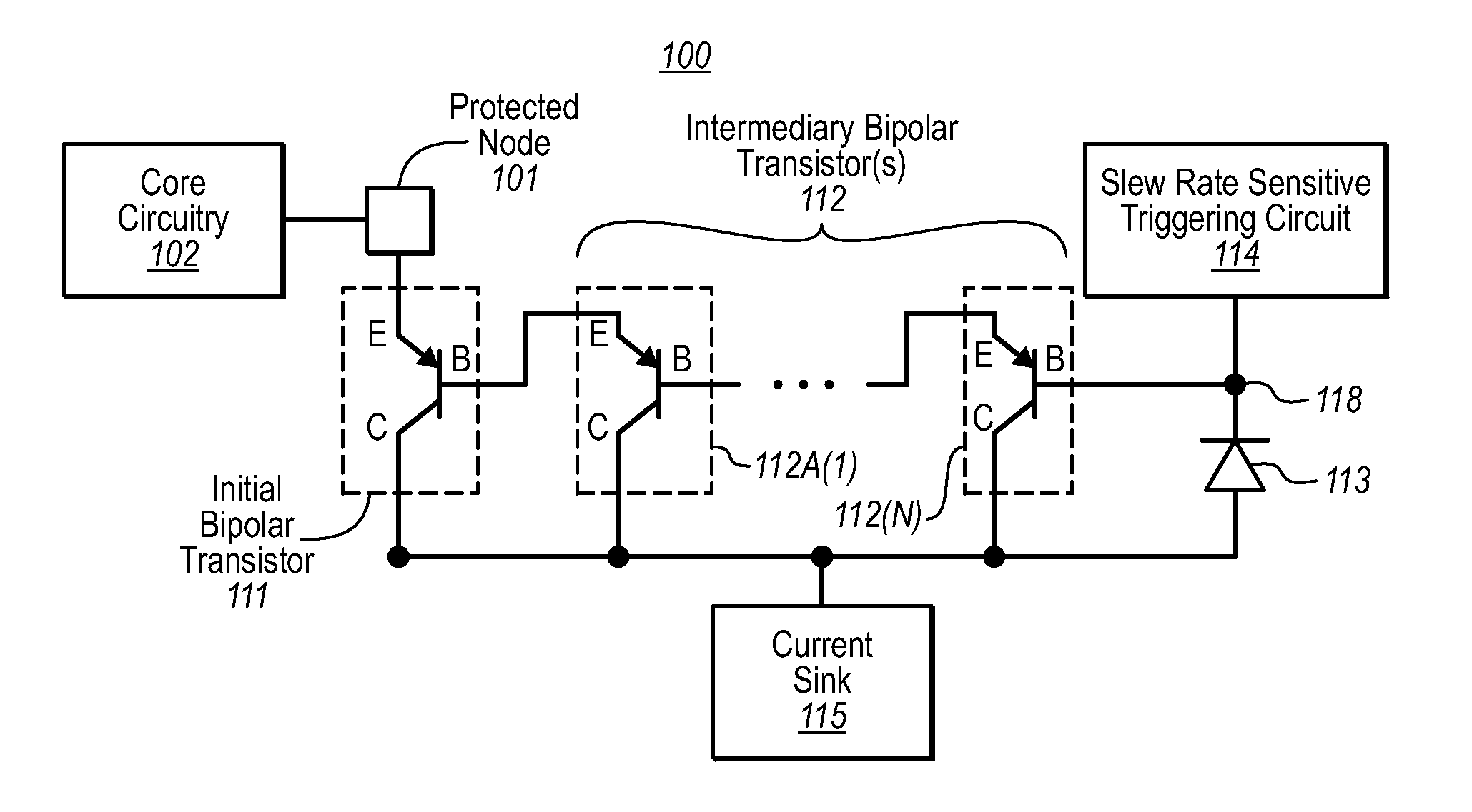
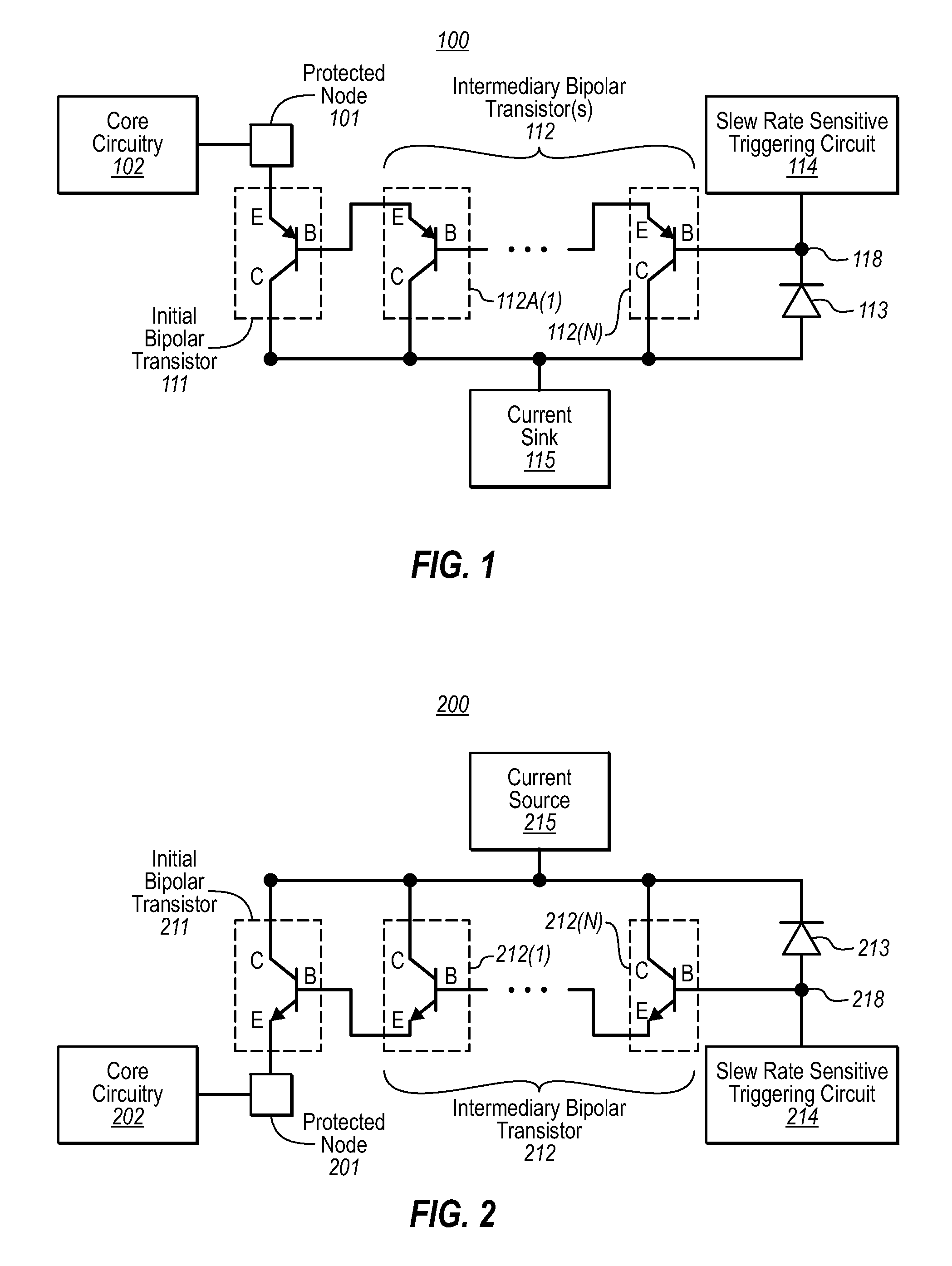
[0015]Embodiments of the present invention relate to the use of a current protection circuit configured to provide current protection to a circuit node through a sequence of two or more bipolar transistors and a final reverse-biased diode. FIG. 1 illustrates an example embodiment in which the sequence of bipolar transistors includes PNP bipolar transistors, whereas FIG. 2 illustrates an example embodiment in which the sequence of bipolar transistors includes NPN bipolar transistors.

[0016]A current protection circuit protects a circuit node from experiencing excessive voltages thereby protecting core circuitry that is coupled to the protected circuit node. For instance, the current protection circuitry 100 of FIG. 1 shows a protected node 101 that is coupled to core circuitry 102. The remainder of the current protection circuitry 100 is configured to draw an appropriate amount of current from the protected node 101 so as to keep the protected node 101 from experiencing excessively hi...


PUM


Abstract

A current protection circuit that uses a sequence of bipolar transistors to provide or draw current from a protected circuit node. An initial bipolar transistor has its emitter terminal coupled to the protected circuit node, with its collector terminal coupled to a current source or sink. One or more additional intermediary bipolar transistors are also provided in the sequence. Each additional intermediary bipolar transistor has its emitter terminal coupled to the base terminal of the previous bipolar transistor in the sequence, and has its collector terminal coupled to the current source or sink. To complete the sequence, a reverse-biased diode is coupled between the base terminal of the final intermediary bipolar transistor and the current source or sink. This allows for effective triggering of current protection for a protected circuit node without requiring a zener diode.

Description

BACKGROUND[0001]Electronic circuitry provides complex functionality that is proving ever more useful. In one common form, circuitry is formed on a semiconductor or other substrate using micro-fabrication processing technology. Typically, circuits with small feature dimension sizes are not designed to carry large amounts of current. So long as the voltage range at any given node does not extend outside of its designed range, these currents remain relatively low and the circuitry will typically operate as designed. However, if the voltage range at any given node extends out of its designed range, a condition of Electrical OverStress (EOS) may occur.[0002]For example, most common semiconductor fabrication processes use substrate or bulk semiconductor with different dopants implanted into certain regions of the substrate. These implant regions define unique electrical characteristics that are important or essential for circuit functionality. Thus, EOS experienced at any of the implant r...

Claims


Application Information

Patent Timeline
Patent Type & Authority Patents(United States)
IPC IPC(8): H02H3/20H02H9/04H02H9/00
CPCH01L27/0259
Inventor TYLER, MATTHEW A.NAUGHTON, JOHN J.
Owner SEMICON COMPONENTS IND LLC
Why Eureka
Try Eureka