Semiconductor device having a round-shaped nano-wire transistor channel and method of manufacturing same

a nano-wire transistor and semiconductor device technology, applied in the field of field-effect transistors, can solve the problems of limited number of spaced channel layers in these conventional devices, too narrow channel width, and inability to perform fast operations

Active Publication Date: 2010-01-05
SAMSUNG ELECTRONICS CO LTD
View PDF26 Cites 59 Cited by
  • Summary
  • Abstract
  • Description
  • Claims
  • Application Information

AI Technical Summary

Benefits of technology

[0046]According to the invention, a round-shaped (circular) nano-wire channel is produced in a FET using an etching process and an annealing process using H2. This process of manufacturing the FET reduces an electric field concentration phenomenon that occurs at the corner of a conventional FET having a square-shaped nano-wire channel. In producing the round-shaped nano-wire channel, the H2 annealing is done at relatively low temperature. Annealing at high temperature results in a nano-wire whose shape can result in the FET channel being cut or interrupted due to a silicon migration effect. Also, an uppermost silicon germanium layer used as a sacrificial layer can have a higher percentage of germanium than the other layers. This results in preventing the uppermost silicon channel layer from being consumed during etching. A damascene process can be used to form a self-aligned transistor gate.

Problems solved by technology

However, in the case of a device using a STI (Shallow Trench Isolation), a channel width that is too narrow may decrease a threshold voltage.
Each of these conventional devices and the corresponding methods of fabricating these devices, suffer from one of more disadvantages.
For example, these conventional devices are limited in an ability to perform fast operations.
Moreover, the number of spaced channel layers in these conventional devices is limited due to fabrication limitations, e.g., with respect to an etching depth that can be achieved during dry etching.

Method used


Image

  • Semiconductor device having a round-shaped nano-wire transistor channel and method of manufacturing same
  • Semiconductor device having a round-shaped nano-wire transistor channel and method of manufacturing same
  • Semiconductor device having a round-shaped nano-wire transistor channel and method of manufacturing same

Examples


Embodiment Construction

[0063]In the following detailed description, when a layer is described as being formed on another layer or on a substrate, the layer may be formed on the other layer or on the substrate, or a third layer may be interposed between the layer and the other layer or the substrate.

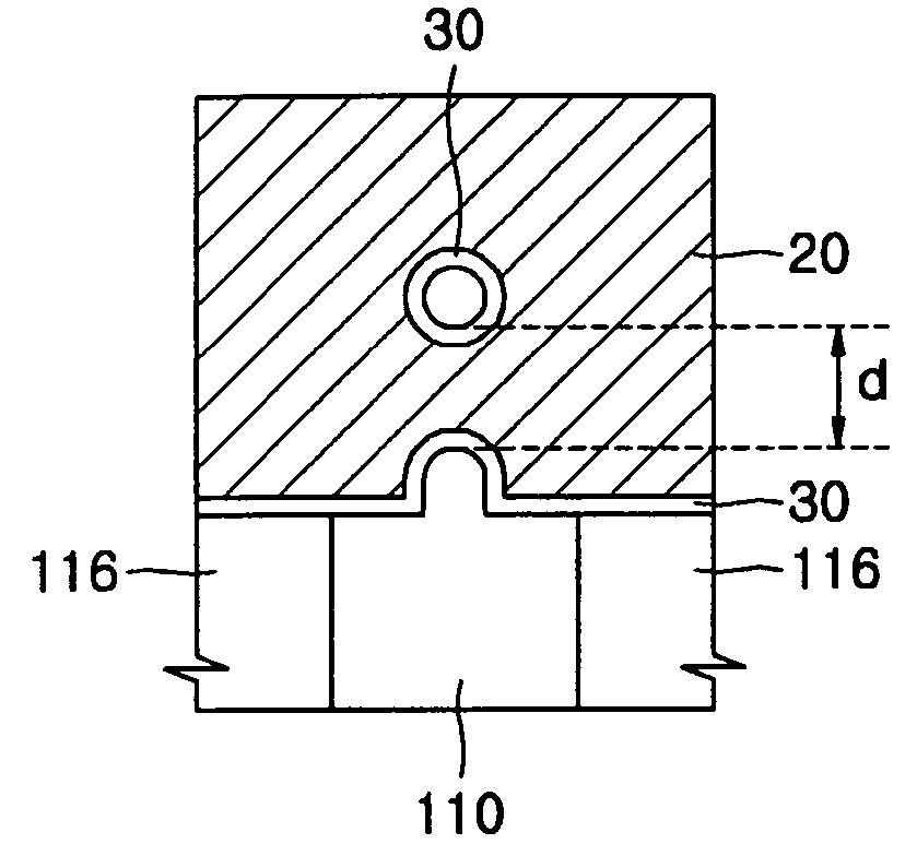
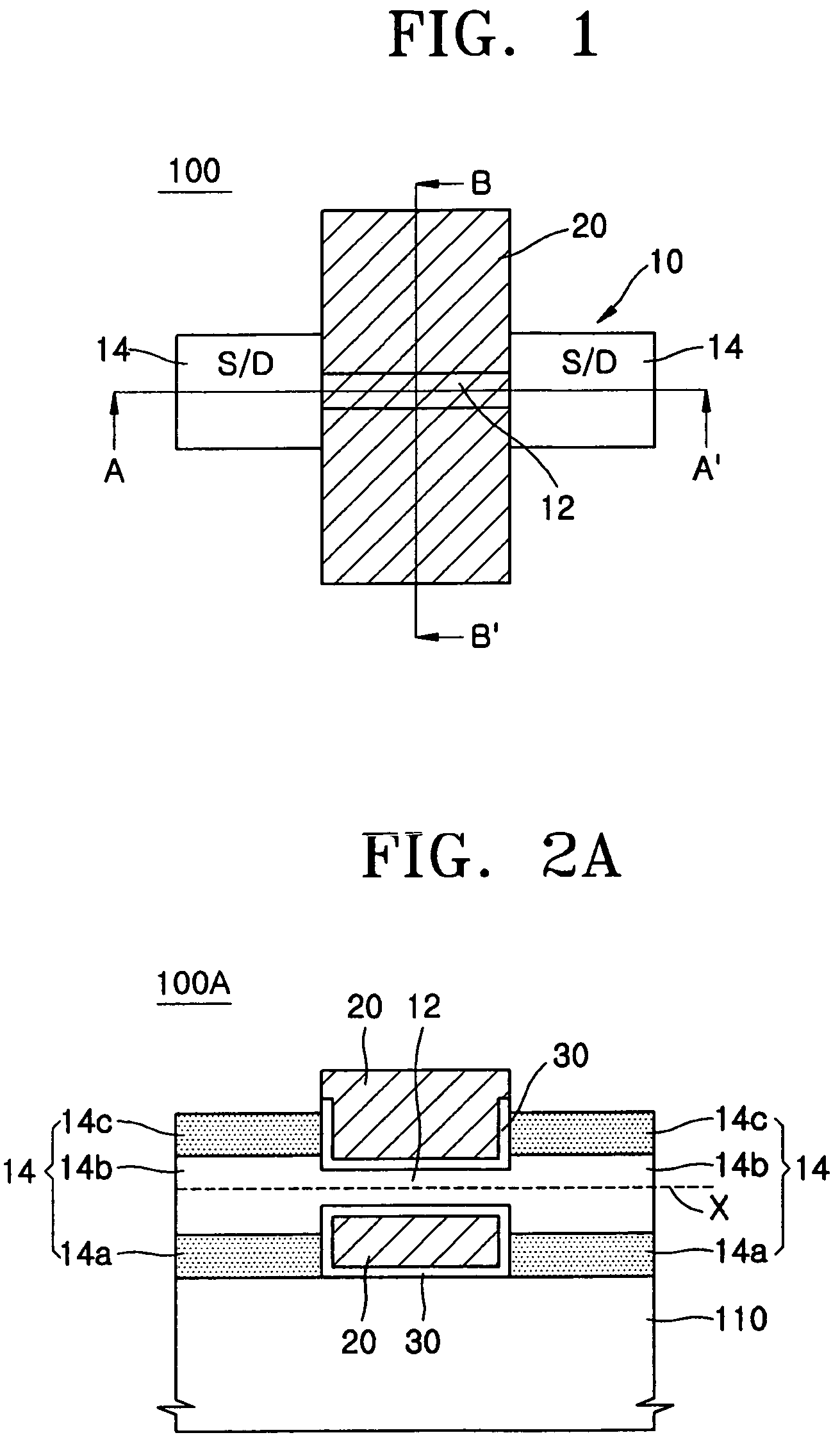
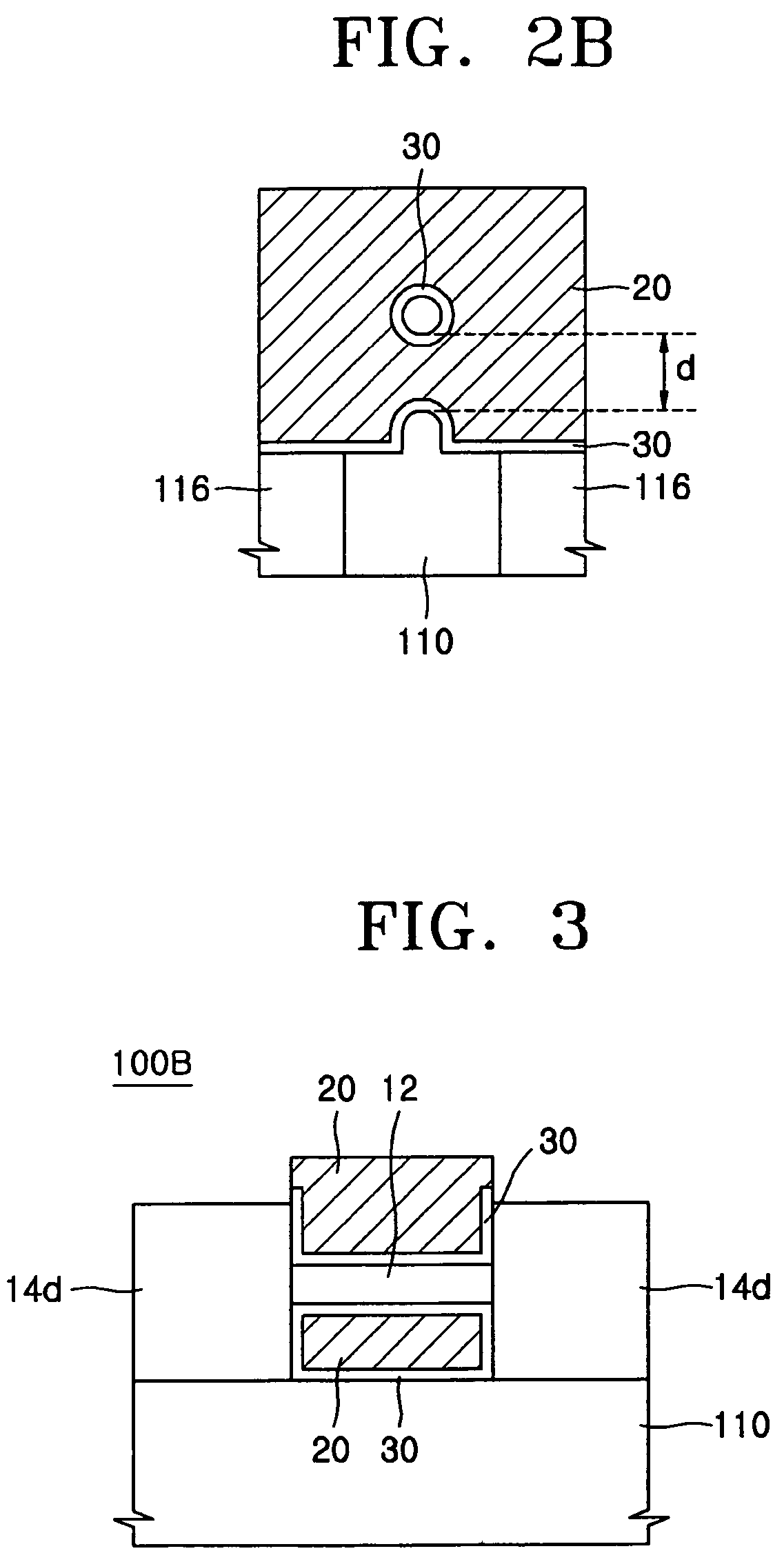
[0064]FIG. 1 is a schematic top plan view of a FET with a round or circular shaped nano-wire channel in accordance with an embodiment of the invention. FIG. 2A is a schematic cross-sectional view of one embodiment of the FET of FIG. 1, taken along line A-A′ of FIG. 1. FIG. 2B is a schematic cross-sectional view of the embodiment of the FET of FIG. 2A taken along line B-B′ of FIG. 1.

[0065]Referring to FIGS. 1, 2A and 2B, the FET structure of the invention includes a semiconductor substrate 110. Source / drain regions 14 are formed on the substrate 110, the source / drain regions 14 include a stacked structure of a first silicon germanium (SiGe) layer 14a, a silicon layer 14b and a second SiGe layer 14c sequentially ...


PUM


Abstract

A field-effect transistor (FET) with a round-shaped nano-wire channel and a method of manufacturing the FET are provided. According to the method, source and drain regions are formed on a semiconductor substrate. A plurality of preliminary channel regions is coupled between the source and drain regions. The preliminary channel regions are etched, and the etched preliminary channel regions are annealed to form FET channel regions, the FET channel regions having a substantially circular cross-sectional shape.

Description

RELATED APPLICATION[0001]This application relies for priority on Korean patent application number 2005-0024543, filed in the Korean Intellectual Property Office on Mar. 24, 2005, the contents of which are incorporated herein by reference in their entirety.FIELD OF THE INVENTION[0002]The invention relates to field-effect transistors (FETs) on semiconductor substrates and manufacturing methods thereof, and, more particularly, to a FET having a round-shaped, i.e., circular, nano-wire channel and a fabricating method thereof.DESCRIPTION OF THE RELATED ART[0003]As applications for semiconductor devices expand, highly-integrated and / or high-speed semiconductor devices are increasingly in demand. As integration density of semiconductor devices increases, a design rule becomes smaller. As a result of the decreasing design rule, a channel length and a channel width of a field effect transistor (FET) similarly decrease. A decrease in channel length may result in a short channel effect. A decr...

Claims


Application Information

Patent Timeline
Patent Type & Authority Patents(United States)
IPC IPC(8): H01L29/78
CPCB82Y10/00H01L29/045H01L29/0665H01L29/0673H01L29/7854H01L29/42392H01L29/66772H01L29/66795H01L29/42384H01L29/66787H01L29/78696H01L21/18B82Y40/00
Inventor LEE, SUNGYOUNGSHIN, DONGSUK
Owner SAMSUNG ELECTRONICS CO LTD
Why Eureka
Try Eureka