System and method for providing a low voltage thin gate input/output structure with thick gate overvoltage/backdrive protection

a technology of overvoltage/backdrive protection and thin gate input/output structure, which is applied in the direction of pulse automatic control, pulse manipulation, pulse technique, etc., can solve the problems of limiting the alternating current (ac) performance of the input/output structure, affecting the efficiency and affecting the quality of the pmos transistor

Active Publication Date: 2010-01-05
NAT SEMICON CORP
View PDF8 Cites 4 Cited by
  • Summary
  • Abstract
  • Description
  • Claims
  • Application Information

AI Technical Summary

Problems solved by technology

The inability to completely turn off native and depletion NMOS transistors often prevents the native and depletion NMOS transistors from being used in standard logic gates and other circuits.
This requirement gives rise to problems in providing robust electrostatic discharge (ESD) performance and acceptable alternating current (ac) performance.
A major problem with this approach is that at room temperature (about twenty three degrees Celsius (23° C.)) the threshold voltage (Vth) for a thick gate PMOS transistor is typically nine tenths of a volt (0.9 V).
Therefore, the ability of a PMOS transistor to provide a sufficient drive is severely limited.
First, the special lever shifters will limit the alternating current (ac) performance of the input/output structure.
However, this would provide an undesirable increase in the amount of current consumption in the input/output structure.
One major drawback of the prior art input/output structure 100 shown in FIG. 1 is that the switching transistors (M1 a...

Method used


Image

  • System and method for providing a low voltage thin gate input/output structure with thick gate overvoltage/backdrive protection
  • System and method for providing a low voltage thin gate input/output structure with thick gate overvoltage/backdrive protection
  • System and method for providing a low voltage thin gate input/output structure with thick gate overvoltage/backdrive protection

Examples


Embodiment Construction

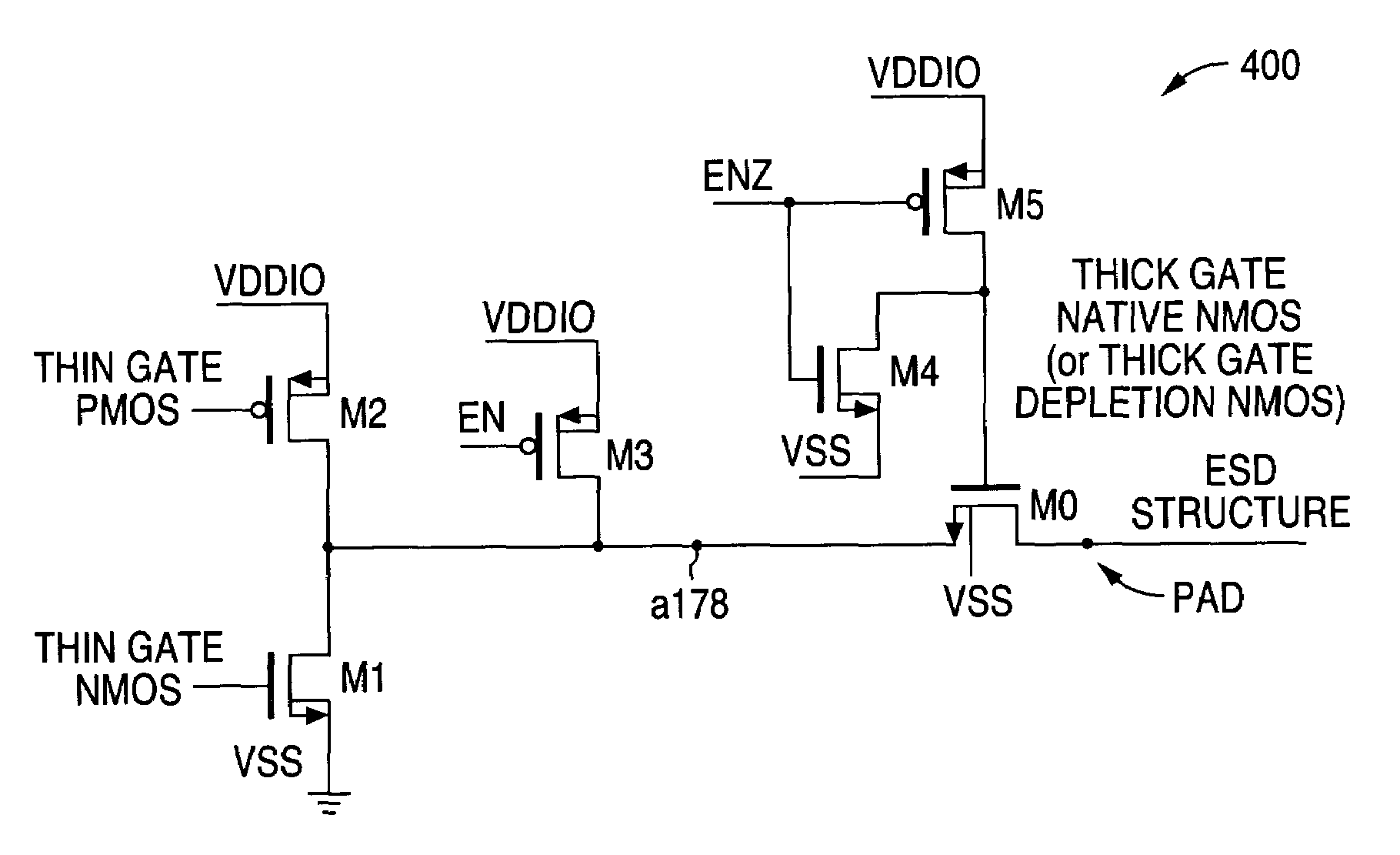
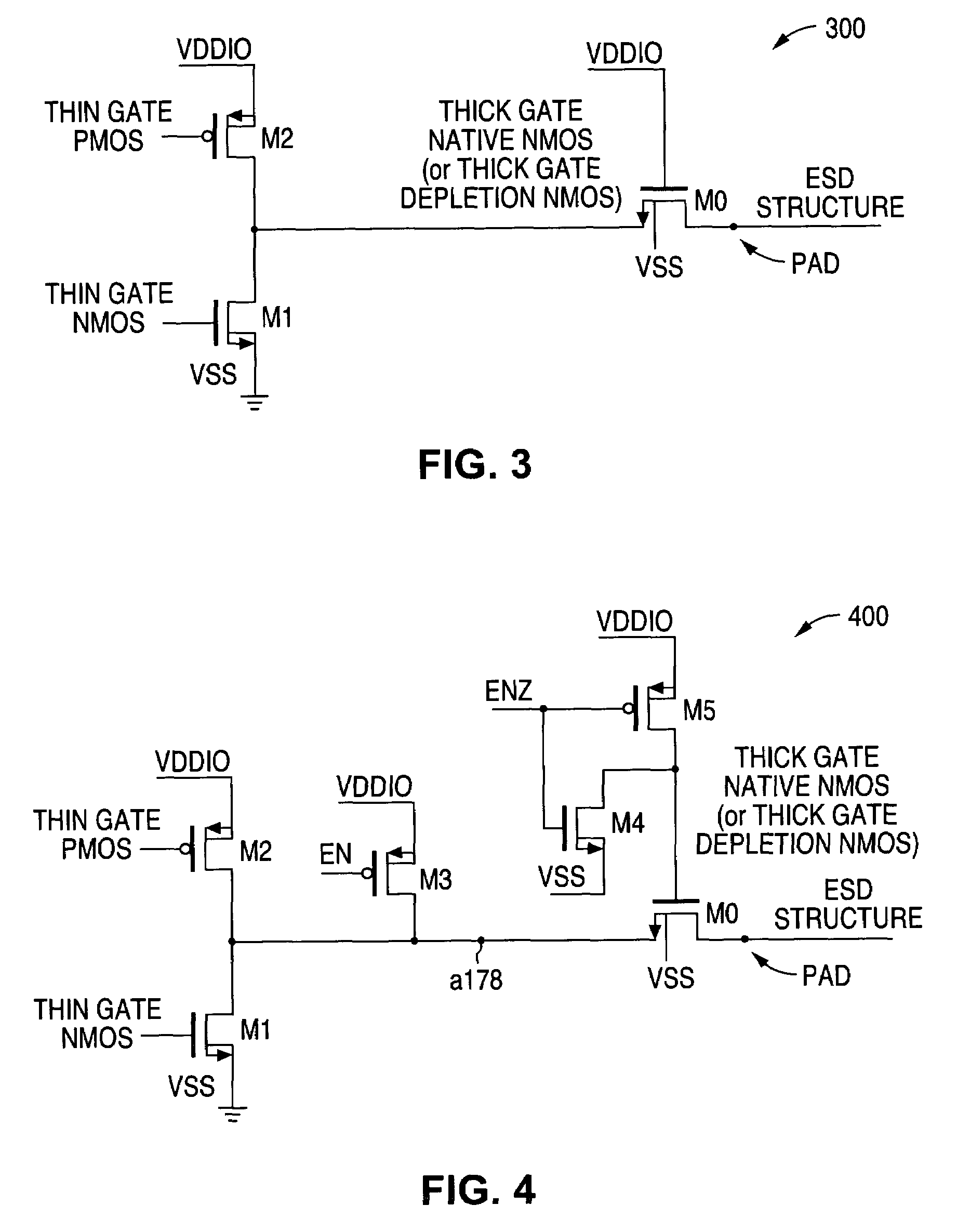
[0040]FIGS. 3 through 11, discussed below, and the various embodiments used to describe the principles of the present invention in this patent document are by way of illustration only and should not be construed in any way to limit the scope of the invention. Those skilled in the art will understand that the principles of the present invention may be implemented with any type of suitably arranged input / output structure for an integrated circuit.

[0041]There are several advantages to be gained if one replaces the transfer gate of an input / output structure with a thick gate native n-channel metal oxide semiconductor (NMOS) transistor. A native NMOS transistor has a threshold voltage (Vth) of approximately a negative one tenth volt (−0.1 V). If the native NMOS transistor is implemented as a thick gate transistor, it is possible to limit the voltage that may be pushed through the native NMOS transistor to a voltage that is equal to approximately three tenths of a volt (0.3 V) plus th...


PUM


Abstract

A system and method are disclosed for providing an integrated circuit low voltage thin gate input/output structure with thick gate overvoltage/backdrive protection. In an advantageous embodiment of the present invention, a transfer gate of the input/output structure comprises at least one thick gate native (or depletion) n-channel metal oxide semiconductor (NMOS) transistor that is connected to an output pad node of the input/output structure. The thick gate native (or depletion) NMOS transistor prevents current from the output pad node from entering the input/output structure when a voltage level of the output pad node is high.

Description

TECHNICAL FIELD OF THE INVENTION[0001]The present invention is generally directed to the manufacture of integrated circuits and, in particular, to providing a low voltage, thin gate input / output structure with thick gate overvoltage / backdrive protection.BACKGROUND OF THE INVENTION[0002]In the manufacture of integrated circuits it is desirable to provide overvoltage / backdrive protection for input / output structures. It is desirable to provide an overvoltage / backdrive protection circuit that is capable of preventing reverse charge leakage and gate oxide breakdown when the voltage on an input / output structure exceeds an internal power supply voltage or when the input / output structure is powered down.[0003]The term “backdrive” refers to a condition that may occur when a device that is powered down is connected to a bus to which other devices are also connected. When one of the other devices is powered up and begins driving the bus, the device that is powered down may receive a “backdrive...

Claims


Application Information

Patent Timeline
IPC IPC(8): H01L23/62
CPCH03K19/00315H01L27/0251
Inventor WERT, JOSEPH D.
Owner NAT SEMICON CORP
Why Eureka
Try Eureka