Low-voltage operational amplifier and operational amplifying method

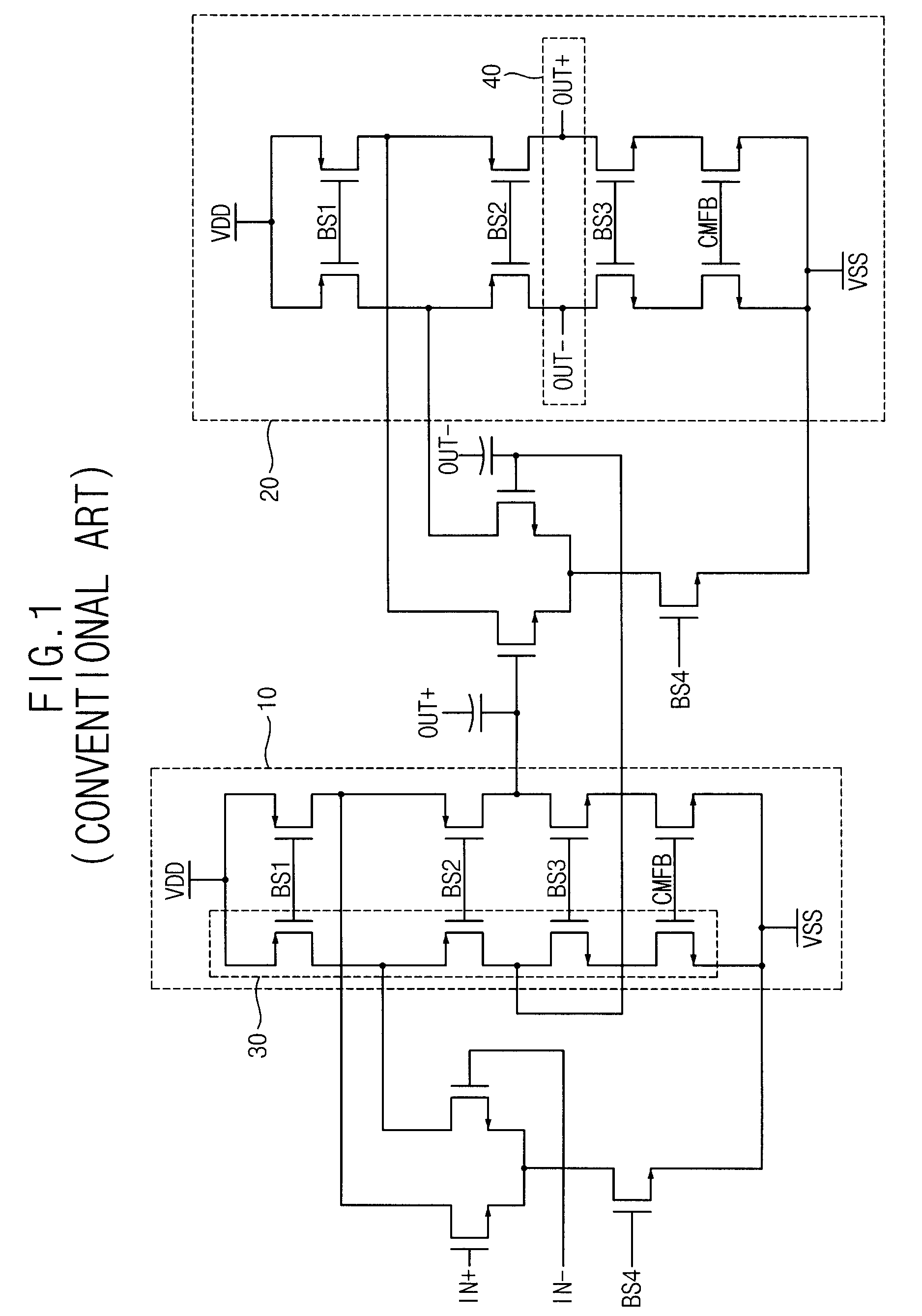
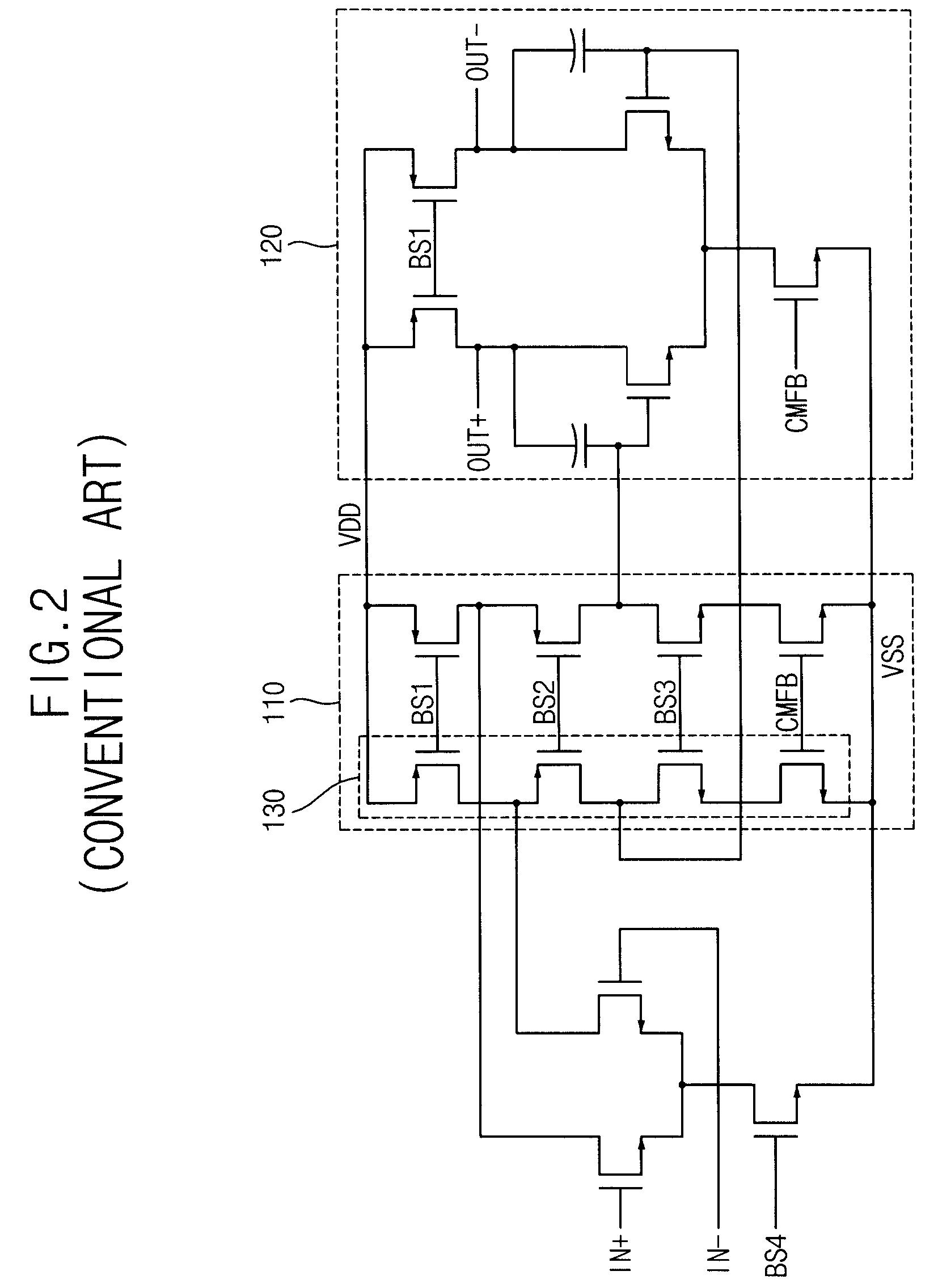
a low-voltage operational amplifier and low-voltage technology, applied in the direction of dc-amplifiers with dc-coupled stages, differential amplifiers, amplifiers, etc., can solve the problems of low power-supply voltage operation that operates properly at a high power-supply voltage, and conventional operational amplifiers of fig. 1 and fig. 2 do not efficiently obtain a large dynamic voltage margin at a relatively low power-supply voltage, so as to redu

Inactive Publication Date: 2010-01-12
SAMSUNG ELECTRONICS CO LTD
View PDF9 Cites 3 Cited by
  • Summary
  • Abstract
  • Description
  • Claims
  • Application Information

AI Technical Summary

Benefits of technology

[0014]Exemplary embodiments of the present invention provide an operational amplifying method capable of reducing a settling time of output signals at a low voltage.
[0015]In exemplary embodiments of the present invention, a low-voltage operational amplifier includes a differential amplifying stage that amplifies a difference between a first signal and a second signal that constitute a differential pair using an input pair of NMOS transistors, and that outputs an amplified first signal and an amplified second signal, an output amplifying stage that amplifies a difference between the amplified first signal and the amplified second signal using an input pair of PMOS transistors, and that outputs a first output signal and a second output signal that constitute a differential pair and a compensation stage that receives the amplified first signal, the amplified second signal, the first output signal, and the second output signal and that reduces a settling time of the first output signal and the second output signal.
[0029]In exemplary embodiments of the present invention, a low-voltage operational amplifier includes a differential amplifying stage that amplifies a difference between a first signal and a second signal that constitute a differential pair using an input pair of PMOS transistors, and that outputs an amplified first signal and an amplified second signal, an output amplifying stage that amplifies a difference between the amplified first signal and the amplified second signal using an input pair of NMOS transistors, and that outputs a first output signal and a second output signal that constitute a differential pair, and a compensation stage that receives the amplified first signal, the amplified second signal, the first output signal, and the second output signal, and that reduces a settling time of the first output signal and the second output signal.
[0043]In exemplary embodiments of the present invention, an operational amplifying method includes amplifying a difference between a first signal and a second signal that constitute a differential pair, outputting an amplified first signal and an amplified second signal, amplifying a difference between the amplified first signal and the amplified second signal, outputting a first output signal and a second output signal that constitute a differential pair, receiving the amplified first signal, the amplified second signal, the first output signal, and the second output signal, and reducing a settling time of the first output signal and the second output signal.
[0044]Accordingly, the low-voltage operational amplifier can have a high gain, a large swing margin, and a fast settling time, and can operate at a low voltage. The operational amplifying method can reduce a settling time of output signals.

Problems solved by technology

Therefore, a circuit that operates properly at a high power-supply voltage may not operate properly at a low power-supply voltage.
Thus, the conventional operational amplifier of FIG. 1 does not efficiently obtain a large dynamic voltage margin at a relatively low power-supply voltage.
Thus, the conventional operational amplifier of FIG. 2 does not efficiently obtain a large dynamic voltage margin at a low power-supply voltage.
In addition, the conventional operational amplifier of FIG. 2 achieves a relatively low gain compared with the other conventional operational amplifier of FIG. 1.

Method used


Image

  • Low-voltage operational amplifier and operational amplifying method
  • Low-voltage operational amplifier and operational amplifying method
  • Low-voltage operational amplifier and operational amplifying method

Examples


Embodiment Construction

[0052]Exemplary embodiments of the present invention now will be described more fully with reference to the accompanying drawings, in which exemplary embodiments of the invention are shown. This invention may, however, be embodied in many different forms and should not be construed as limited to the exemplary embodiments set forth herein. Rather, these exemplary embodiments are provided so that this disclosure will be thorough and complete, and will fully convey the scope of the invention to those of ordinary skill in the art. Like reference numerals refer to like elements throughout this application.

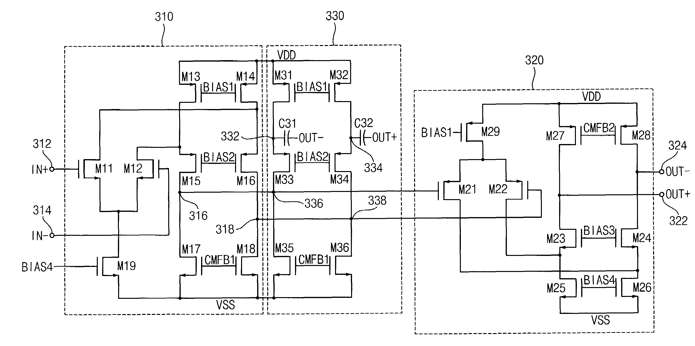
[0053]FIG. 3 is a circuit diagram illustrating a low-voltage operational amplifier according to an exemplary embodiment of the present invention.

[0054]Referring to FIG. 3, the low-voltage operational amplifier includes a differential amplifying stage 310 that includes an input pair of NMOS transistors a differential amplifying stage 320 that includes an input pair of PMOS transistors, a...


PUM


Abstract

A low-voltage operational amplifier includes a differential amplifying stage, an output amplifying stage and a compensation stage. The differential amplifying stage amplifies a difference between a first signal and a second signal that constitute a differential pair using an input pair of NMOS transistors, and outputs an amplified first signal and an amplified second signal. The output amplifying stage amplifies a difference between the amplified first signal and the amplified second signal using an input pair of PMOS transistors, and outputs a first output signal and a second output signal that constitute a differential pair. The compensation stage receives the amplified first signal, the amplified second signal, the first output signal, and the second output signal, and reduces a settling time of the first output signal and the second output signal.

Description

CROSS-REFERENCE TO RELATED APPLICATION[0001]This application claims priority under 35 USC § 119 to Korean Patent Application No. 2006-0107526, filed on Nov. 2, 2006 in the Korean Intellectual Property Office, the disclosure of which is incorporated herein in its entirety by reference.BACKGROUND OF THE INVENTION[0002]1. Technical Field[0003]The present disclosure relates to an operational amplifier and, more particularly, to a low-voltage operational amplifier and an operational amplifying method.[0004]2. Discussion of Related Art[0005]As techniques in a semiconductor manufacturing process are improved, the width between the semiconductor circuit lines is gradually decreased. Because the width between the semiconductor circuit lines becomes narrower, an integration degree of the semiconductor is improved and a production cost of the semiconductor is reduced. In addition, as the width between the semiconductor circuit lines gradually becomes narrower, a power-supply voltage that is ap...

Claims


Application Information

Patent Timeline
Patent Type & Authority Patents(United States)
IPC IPC(8): H03F3/45
CPCH03F3/45192H03F2200/513H03F2203/45122H03F2203/45248H03F2203/45302H03F2203/45631H03F2203/45642H03F2203/45652H03F3/45H03F1/22
Inventor LEE, KANG-JINSHIN, EUN-SEOK
Owner SAMSUNG ELECTRONICS CO LTD
Why Eureka
Try Eureka