Memory module comprising a plurality of memory devices
a memory module and memory device technology, applied in the field of memory modules, can solve the problems of inability to ensure the so-called “integrity” of data, and inability to achieve error correction in the event of failure of an entire devi
- Summary
- Abstract
- Description
- Claims
- Application Information
AI Technical Summary
Benefits of technology
Problems solved by technology
Method used
Image
Examples
Embodiment Construction
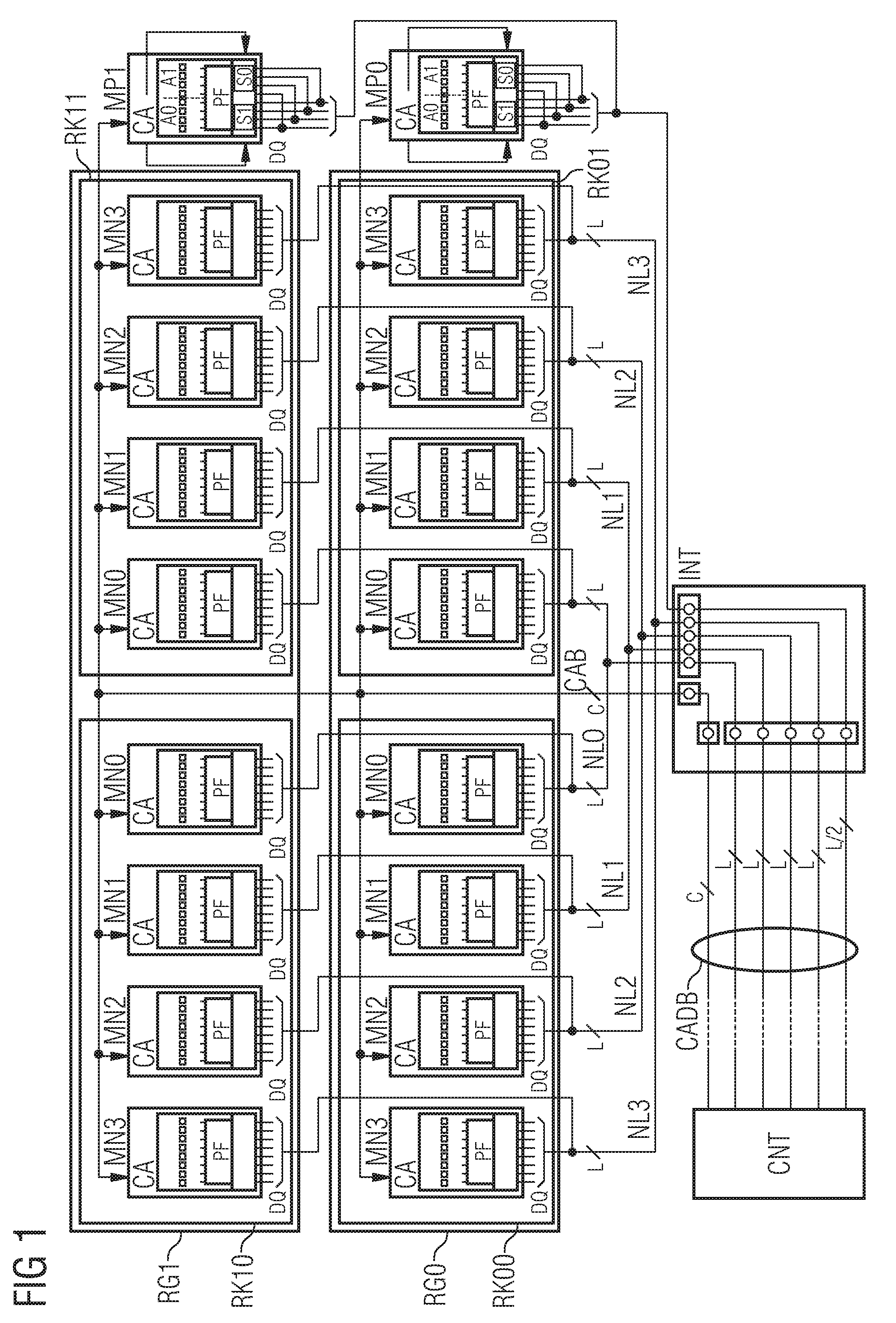
[0035]In FIG. 1, elements of identical type are designated by the same letter combinations each succeeded by a number or number combination for identifying the relevant element. A colon between two numbers denotes the word “to”; thus, e.g. “MN0:3” is to be read as “MN0 to MN3”.
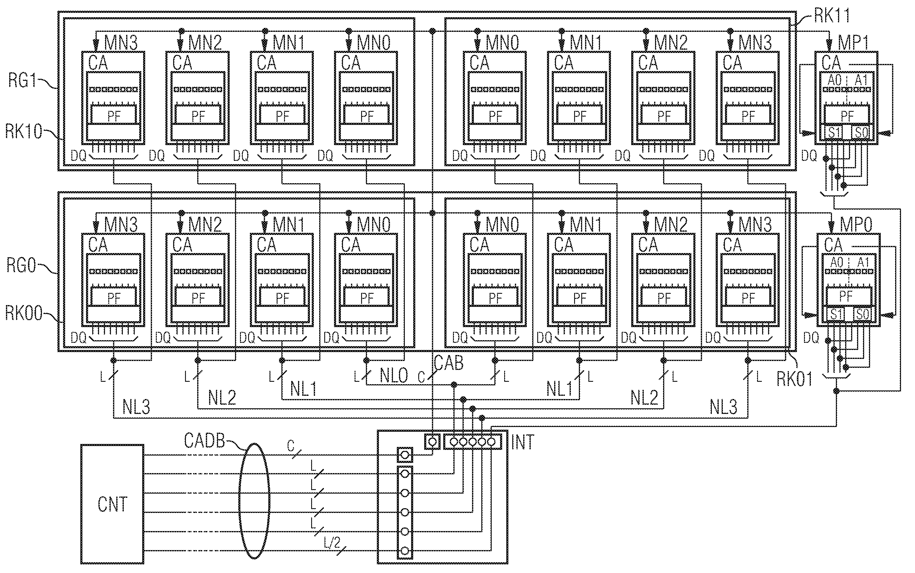
[0036]The memory module illustrated schematically in FIG. 1 contains two rank groups RG0 and RG1, each of which comprises R=2 ranks RK00, RK01 and RK10, RK11, respectively. Each rank contains KN=4 useful bit memory devices MN0:3, each of which has a bidirectional data port DQ with L=8 pins for inputting and outputting a group of L=8 parallel bits which are intended to be written and read at a respectively selected group of L=8 memory cells (L-cell group). The relevant 8-cell group is selected depending on the pattern of a plurality of address bits which are received at assigned pins of a control and address terminal CA. In FIG. 1, in each useful bit memory device, an 8-cell group of this type is symbolically i...
PUM
 Abstract
Description
Claims
Application Information


