Electronic emission device, electron emission display device having the same, and method of manufacturing the electron emission device

a technology of electron emission display and electron emission device, which is applied in the manufacture of electrode systems, electric discharge tubes/lamps, and discharge tubes luminescent screens, etc., can solve the problems of reduced current density, inability to obtain uniform brightness, and display devices that display images using fea-type electron emission devices that have non-uniform brightness, etc., to achieve simple manufacturing, improve the uniform brightness of pixels, and reduce cost

Inactive Publication Date: 2010-01-26
SAMSUNG SDI CO LTD
View PDF7 Cites 32 Cited by
  • Summary
  • Abstract
  • Description
  • Claims
  • Application Information

AI Technical Summary

Benefits of technology

[0017]Aspects of the present invention provide an electron emission device which can uniformly emit electrons and can be simply manufactured at a reduced cost, and a display apparatus having an improved uniform brightness of pixels by using the electron emission device.
[0018]Aspects of the present invention also provide a simple method of manufacturing the electron emission device.

Problems solved by technology

A display device that displays an image using an FEA type electron emission device often has non-uniform brightness.
In addition, since the distances between the gate electrode and tips of a carbon nanotube (CNT) in each electron emission source are not uniform, current density is reduced and uniform brightness cannot be obtained.

Method used


Image

  • Electronic emission device, electron emission display device having the same, and method of manufacturing the electron emission device
  • Electronic emission device, electron emission display device having the same, and method of manufacturing the electron emission device
  • Electronic emission device, electron emission display device having the same, and method of manufacturing the electron emission device

Examples


Embodiment Construction

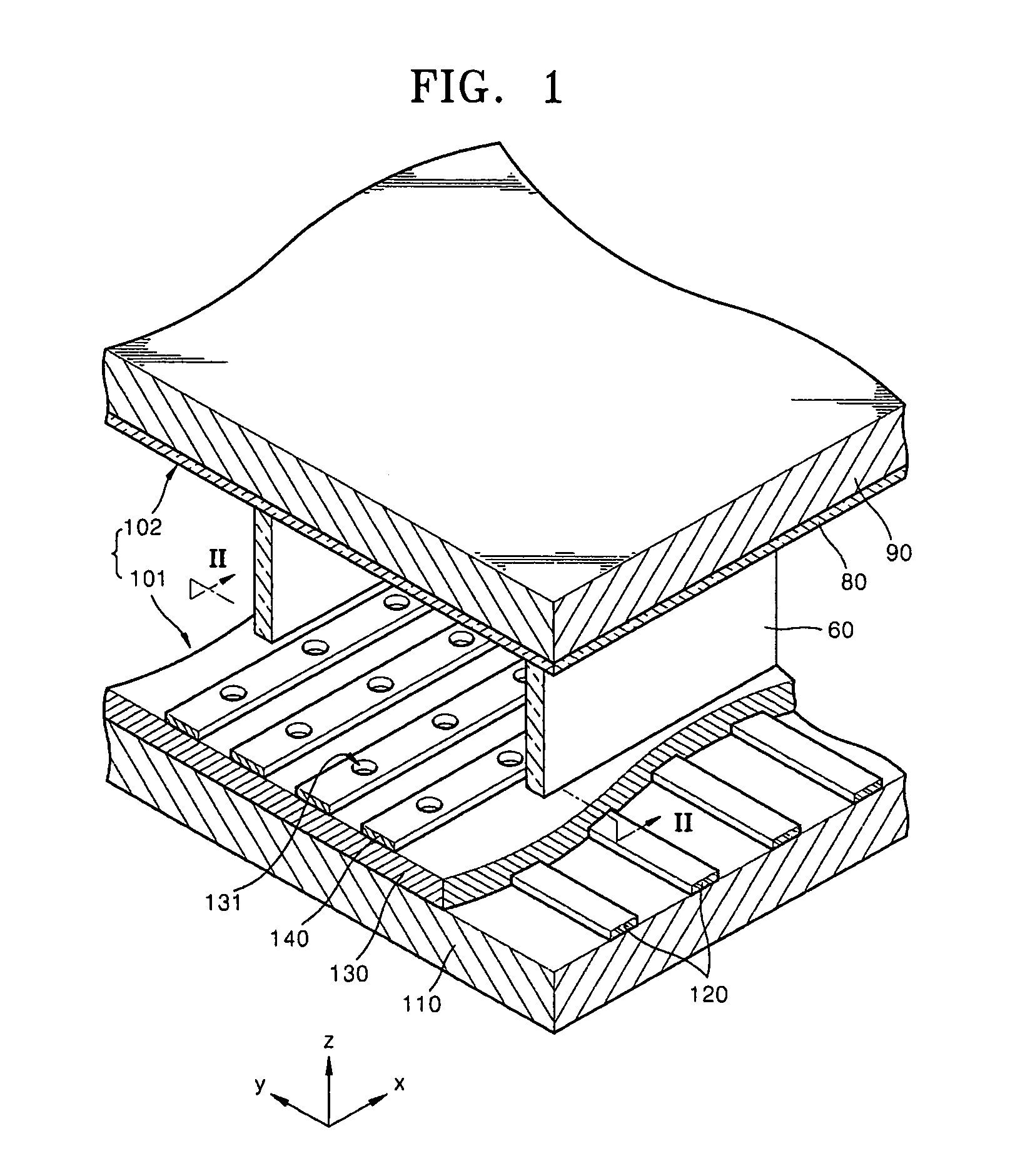
[0032]Reference will now be made in detail to the present embodiments of the present invention, examples of which are illustrated in the accompanying drawings, wherein like reference numerals refer to the like elements throughout. The embodiments are described below in order to explain the present invention by referring to the figures.

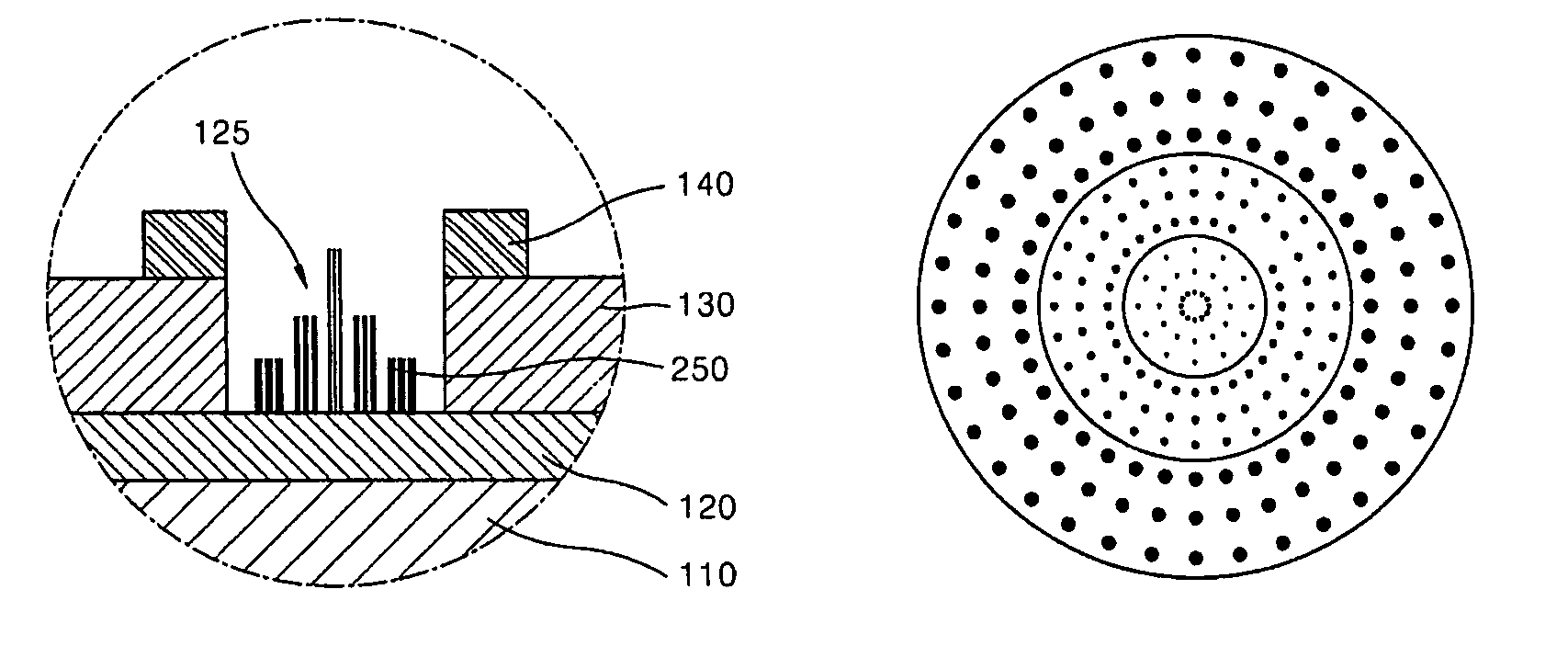
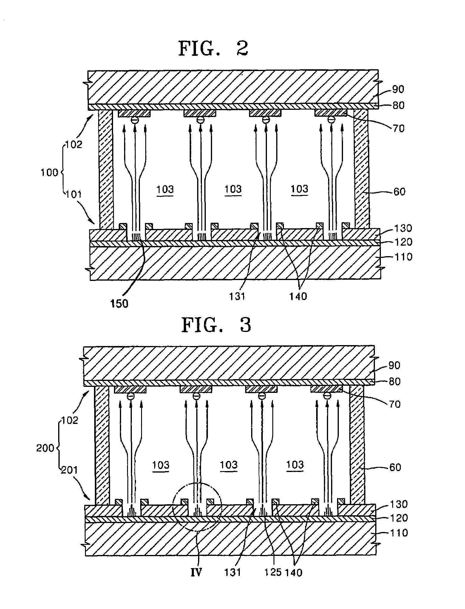
[0033]FIG. 3 is a cross-sectional view of a display device 200 including an electron emission device 201 according to an embodiment of the present invention, and FIG. 4 is an enlarged view of portion IV of FIG. 3.

[0034]Referring to FIGS. 3 and 4, the electron emission device 201 includes a first substrate 110, a cathode electrode 120, a gate electrode 140, a first insulating layer 130, and an electron emission source 125, which comprises a plurality of carbon nanotubes (CNTs) 250.

[0035]The first substrate 110 can be a board having a predetermined thickness, or a glass substrate formed of quartz glass, glass containing a small amount of an impurity such...


PUM


Abstract

An electron emission device which can uniformly emit electrons and can be simply manufactured at a reduced cost, and a display apparatus having improved uniform brightness of pixels by using the electron emission device. In addition, a simple method of manufacturing the electron emission device. The electron emission device includes: a first substrate; a cathode electrode and an electron emission unit disposed on the first substrate; a gate electrode electrically insulated from the cathode electrode; an insulating layer disposed between the cathode electrode and the gate electrode to insulate the cathode electrode from the gate electrode; and an electron emission source including carbon nanotubes (CNTs) that contact the cathode electrode, wherein distances between the gate electrode and the tips of the CNTs are uniform.

Description

CROSS-REFERENCE TO RELATED APPLICATIONS[0001]This application claims the benefit of Korean Patent Application No. 2005-103449, filed on Oct. 31, 2005, in the Korean Intellectual Property Office, the disclosure of which is incorporated herein in its entirety by reference.BACKGROUND OF THE INVENTION[0002]1. Field of the Invention[0003]Aspects of the present invention relate to an electron emission device, an electron emission display apparatus having the electron emission device, and a method of manufacturing the electron emission device, and more particularly, to an electron emission device having a structure in which a voltage applied to an electron emission source is uniformly distributed, an electron emission display apparatus having the electron emission device to increase brightness uniformity of pixels, and a method of manufacturing the electron emission device.[0004]2. Description of the Related Art[0005]Generally, electron emission devices use a thermal cathode or a cold cath...

Claims


Application Information

Patent Timeline
Patent Type & Authority Patents(United States)
IPC IPC(8): H01J1/62H01J1/02H01J1/46H01J21/10H01J63/04H01J9/00H01J9/04H01J9/12H01J9/24
CPCB82Y10/00H01J29/04H01J29/481H01J29/86H01J31/127H01J63/02H01J63/04H01J2201/30469Y10S977/742Y10S977/743Y10S977/765Y10S977/876
Inventor CHOI, YOUNG-CHULPARK, JONG-HWAN
Owner SAMSUNG SDI CO LTD
Why Eureka
Try Eureka