
Correction method of defective pixel in image pickup device and image processing apparatus using the correction method

a technology of image processing apparatus and correction method, which is applied in the direction of television system, color signal processing circuit, instruments, etc., can solve the problems of consuming a large amount of memory space, unable to perform sufficient pixel defect correction, and further degrading in the pixel defect level, so as to achieve the effect of increasing the number of pixel defect data

Inactive Publication Date: 2010-02-02
CANON KK
View PDF4 Cites 25 Cited by
  • Summary
  • Abstract
  • Description
  • Claims
  • Application Information

AI Technical Summary

Benefits of technology

This approach maintains high image quality over time by accurately updating and correcting defective pixels, reducing memory consumption and improving defect level determination efficiency.

Problems solved by technology

The known techniques are unable to perform sufficient pixel defect correction because no defect information is updated concerning a defective pixel that has escaped detection performed before shipment and a defective pixel taking place as a result of aging.
No pixel defect level information updating is performed concerning a defective pixel that was detected at the shipment and further degraded in the pixel defect level subsequent to the shipment.
Since the defective pixel detection is not performed with a desired pixel defect detection level range selected, pixel defect data more than necessary is collected, thereby consuming a large amount of memory space.

Method used


Image

  • Correction method of defective pixel in image pickup device and image processing apparatus using the correction method
  • Correction method of defective pixel in image pickup device and image processing apparatus using the correction method
  • Correction method of defective pixel in image pickup device and image processing apparatus using the correction method

Examples


first embodiment

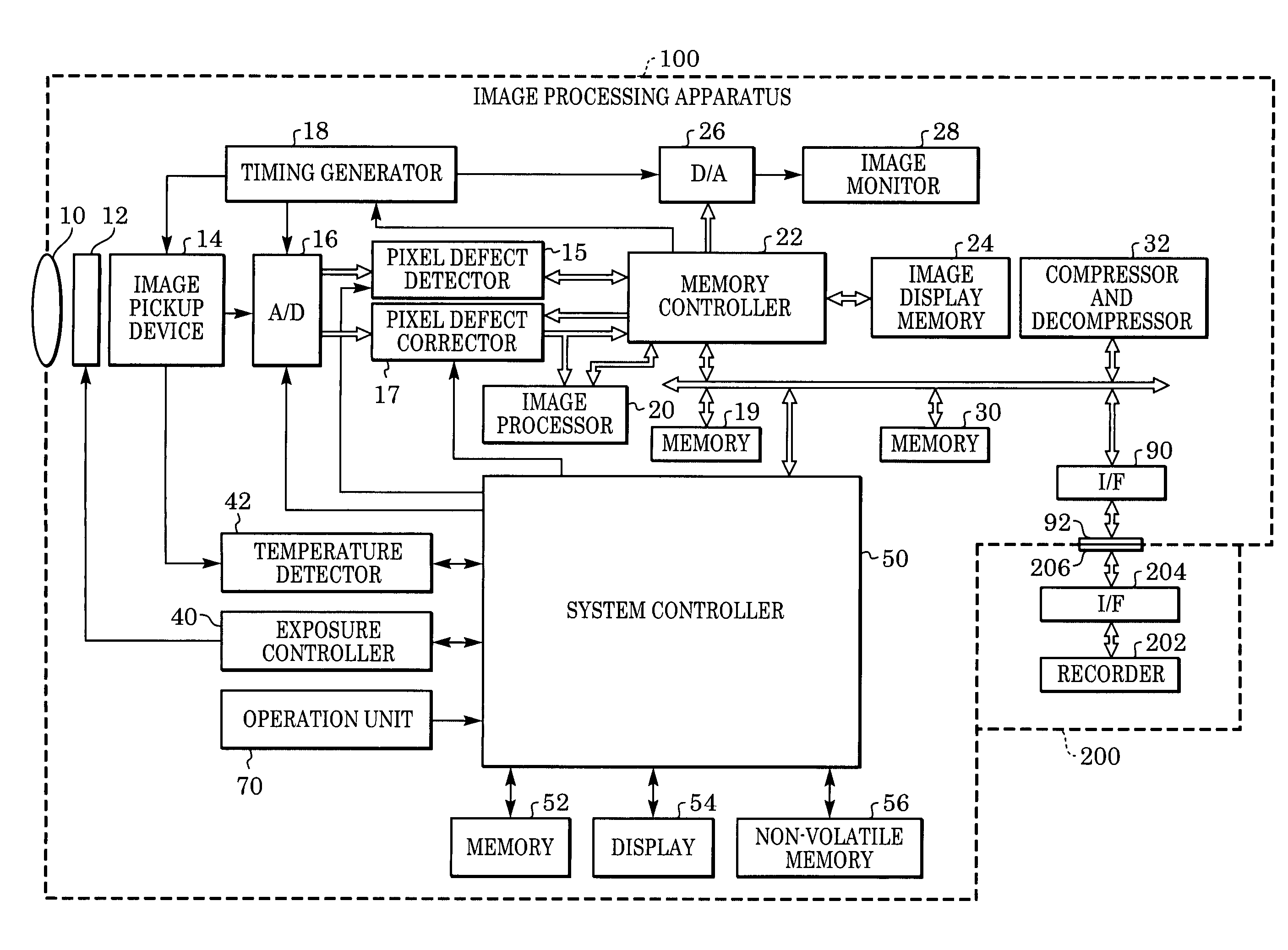
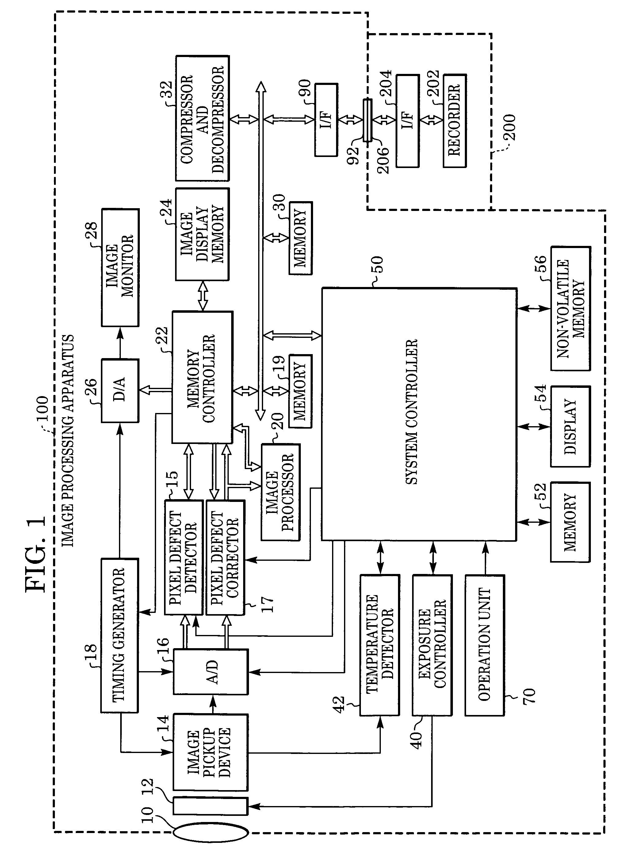
[0031]FIG. 1 is a block diagram illustrating an image processing apparatus 100 having a pixel defect detection and correction function in accordance with a first embodiment of the present invention. The image processing apparatus 100 is an electronic still camera, an electronic video camera, or the like.

[0032]The image processing apparatus 100 includes an imaging lens 10, a shutter 12 having an aperture stop function, a image pickup device 14 for converting an optical image into an electrical signal, and an analog-to-digital (A / D) converter 16 for gain controlling an analog signal from the image pickup device 14 and then analog-to-digital converting the analog signal into a digital signal. By controlling gain, a system controller 50 substantially controls gain of the image processing apparatus 100. The image pickup device 14 includes a two-dimensional matrix of pixels, such as charge-coupled device (CCD) elements, and may contain a defective pixel.

[0033]Upon receiving an image signa...

second embodiment

[0063]A second embodiment of the present invention is identical in structure to the first embodiment of the present invention. The operation of the pixel defect data updating circuit 402 in the second embodiment is described with reference to FIG. 8 and the sensor image of FIG. 5. The pixel defect data updating circuit 402 of the second embodiment has two operation modes. During a first operation mode, the pixel defect data updating circuit 402 operates in the same manner as in the first embodiment of the present invention.

[0064]A second operation mode of the pixel defect data updating circuit 402 is discussed below. The pixel defect data updating circuit 402 compares the detected pixel defect data from the pixel defect determining circuit 400 with the pixel defect data stored beforehand in the memory 19 to update the pixel defect data. As shown in FIG. 5, a number in a circle represents a defective pixel already detected at the time of the shipment of the image processing apparatus...

third embodiment

[0076]A third embodiment of the present invention is described below. FIG. 11 is a block diagram of a digital still camera in accordance with the third embodiment of the present invention. The third embodiment is applicable not only to a digital still camera but also to a video camera or the like.

[0077]As shown in FIG. 11, the digital still camera includes a CCD image pickup device 101, a CDS-A / D (correlated double sampling analog to digital) converter 102 for analog-to-digital converting an image signal of the CCD image pickup device 101, a memory 103 for temporarily storing an image, a JPEG (Joint Photographic Experts Group) compressor 104 for performing JPEG compression, and a digital signal processing (DSP) circuit 105 for signal processing image data.

[0078]Also included in the still camera are a memory controller 106 for controlling memories, a digital-to-analog (D / A) converter 107, a color liquid-crystal display 108, a shutter switch 109, a system controller 110, a card memory...


PUM


Abstract

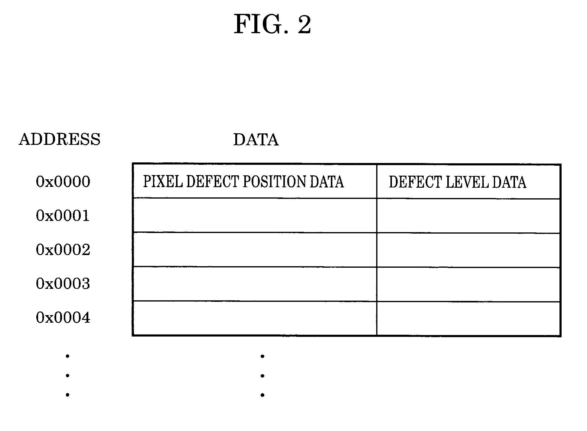
Location information representing the location of a defective pixel in an image pickup device and pixel defect level information representing the pixel defect level of the defective pixel are stored beforehand in a memory. The defect level of the defective pixel is determined after shipment of the image pickup device, and the pixel defect information is updated based on the defect determination result. If a new defective pixel is detected at a location different from the location of the defective pixel with the pixel defect information stored in the memory, the pixel defect information of that defective pixel is added. If a defective pixel is detected at the same location as the defective pixel with the pixel defect information stored in the memory, and if the defect level of the detected defective pixel is worse than the original defect level, the defect level of the defective pixel is updated.

Description

CROSS REFERENCE TO RELATED APPLICATIONS[0001]This application claims priority from Japanese Patent Application Nos. 2003-356442 filed Oct. 16, 2003, and 2003-349594 filed Oct. 8, 2003, which are hereby incorporated by reference herein.BACKGROUND OF THE INVENTION[0002]1. Field of the Invention[0003]The present invention relates to an image processing apparatus and an image processing method using an image pickup device, such as a charge-coupled device (CCD) and, in particular, to a pixel defect correction technique for the image pickup device.[0004]2. Description of the Related Art[0005]The importance of pixel defect correction in the image pickup device is mounting along with high-definition design implemented in the image pickup device for electronic still cameras or video cameras. A variety of techniques for correcting image degradation attributed to an image output from a defective pixel are known. Most of the known techniques correct a defective pixel based on pixel defect infor...

Claims


Application Information

Patent Timeline
Patent Type & Authority Patents(United States)
IPC IPC(8): H04N9/64G02B3/00H04N5/217H04N5/367H04N5/372H04N5/378
CPCH04N5/367H04N5/3675H04N25/683H04N25/68
Inventor MATSUOKA, MASAAKIUDAGAWA, YOSHIRO
Owner CANON KK
Learn More