
Wafer inspection apparatus and wafer inspection method

Active Publication Date: 2021-04-22
HITACHI HIGH-TECH CORP
View PDF0 Cites 0 Cited by
  • Summary
  • Abstract
  • Description
  • Claims
  • Application Information

AI Technical Summary

Benefits of technology

The patent text explains how to fix distortion in a camera image caused by the shape of a wafer, and how to get a clear image for inspection purposes. The technical effect is improved image quality for TDI cameras.

Problems solved by technology

Presence of foreign matters, scratches, crystal defects and the like on the wafer may lead to a defect of a manufactured device.
However, since the TDI camera takes images while moving the wafer, when the wafer has warpage, an image is distorted due to an effect of an inclination of a measurement position and height variation.

Method used


Image

  • Wafer inspection apparatus and wafer inspection method
  • Wafer inspection apparatus and wafer inspection method
  • Wafer inspection apparatus and wafer inspection method

Examples


first embodiment

(1) First Embodiment

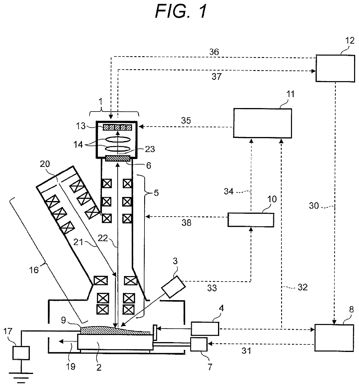
[0028]FIG. 1 is a view illustrating a cross-sectional configuration example of a wafer inspection apparatus using a mirror electron microscope according to a first embodiment. In FIG. 1, an incident electron beam 21 generated by an electron source 20 is made a parallel beam having a large diameter by an irradiation optical system 16 to be incident on a surface of a wafer 9. On a stage 2 on which the wafer 9 is placed, negative potential is applied to the wafer 9 by a negative potential applying power source 17 so as to bounce the incident electron beam 21, and the electron beam is reflected by the wafer surface. The reflected electrons are condensed by an imaging optical system 5 as a reflected electron beam 22 to be incident on a fluorescent plate 6. The fluorescent plate 6 converts the same into light 23 proportional to electron beam density. The light may be infrared light, visible light, ultraviolet light, vacuum ultraviolet light, X-ray and the like dependin...

second embodiment

(2) Second Embodiment

[0057]FIG. 7 is a view illustrating a cross-sectional configuration example of a wafer inspection apparatus using a mirror electron microscope according to a second embodiment. In FIG. 7, components 1 to 38 are the same as those in FIG. 1. The wafer inspection apparatus according to the second embodiment is provided with a height data buffer 110 unlike the wafer inspection apparatus according to the first embodiment (FIG. 1). The buffer 110 temporarily stores to save past height data.

[0058]FIG. 8 is a view illustrating a trajectory 111 of inspection on a wafer. The inspection of a wafer 9 is performed by taking images with a TDI camera 1 while moving a stage 2 in an up-and-down direction. When the images are taken up to a wafer edge, the stage 2 temporarily stops and moves in a horizontal direction on a paper surface by an amount of about one visual field of the TDI camera 1, and moves again in an opposite direction, then the image is taken. Herein, for example,...

third embodiment

(3) Third Embodiment

[0059]FIG. 9 is a view illustrating a cross-sectional configuration example of a wafer inspection apparatus using a mirror electron microscope according to a third embodiment. In FIG. 9, components 1 to 38 are the same as those of the wafer inspection apparatus according to the first embodiment (FIG. 1). However, the wafer inspection apparatus according to the third embodiment is different from the wafer inspection apparatus of the first embodiment (FIG. 1) in that two height sensors are installed and heights of at least two points in a stage advancing direction of an observation position may be measured. Note that, in this embodiment, an example in which the two height sensors are provided is illustrated, but it is also possible to provide three or more height sensors and approximate an observation plane 300 on the basis of respective measurement results.

[0060]FIG. 10 is a view for illustrating observation plane calculation processing by measuring heights of two...


PUM


Abstract

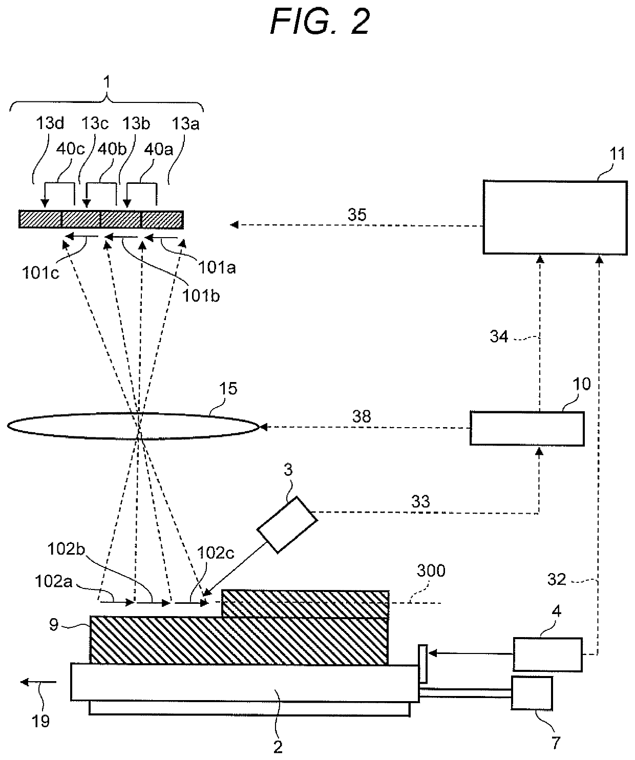
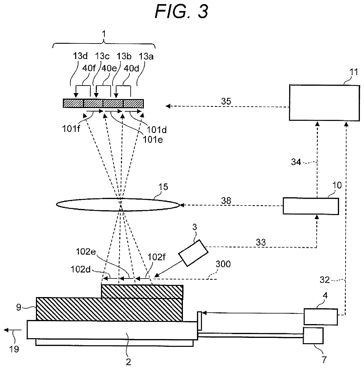
The present disclosure provides a wafer inspection technology that involves less degradation of the image quality even when an object to be observed has a variation in height due to warpage, etc. of a wafer. This wafer inspection apparatus obtains an image with less degradation by: adjusting the focal point of an observation optical system to a height measured by a height sensor for measuring wafer surface heights; and further, correcting a switching signal for a CCD line sensor on the basis of stage position data and optical magnification data corresponding to the height so as to make a correction corresponding to the wafer surface height.

Description

TECHNICAL FIELD[0001]The present disclosure relates to, for example, a wafer inspection apparatus and a wafer inspection method for inspecting a wafer used in an electronic device.BACKGROUND ART[0002]When manufacturing a semiconductor device, a minute device is formed on a wafer made of mirror-polished Si, SiC and the like. Presence of foreign matters, scratches, crystal defects and the like on the wafer may lead to a defect of a manufactured device. In order to reduce a defective rate of the manufactured devices, it is important to inspect a surface of the wafer during a manufacturing process and control each manufacturing process. Therefore, there is an attempt to inspect an entire surface of a wafer with an optical wafer inspection apparatus capable of applying light and laser to observe foreign matters and scratches on the wafer surface by reflective light thereof, and recently with a wafer inspection apparatus applying a mirror electron microscope capable of uniformly applying ...

Claims


Application Information

Patent Timeline
IPC IPC(8): H01L21/67G06T7/64G06T7/00H04N5/235G01N21/95G01N23/2251G01B11/06
CPCH01L21/67288G06T7/64G06T7/0004H04N5/2352G01N21/9505G01N23/2251G01N2223/6116G06T2207/30148G06T2207/10061G01N2223/07G01N2223/20G01N2223/507G01B11/0608H01L22/12G03F7/70625H04N23/72
Inventor DOI, AKIRASASAKI, MINORUHASEGAWA, MASAKIOGAWA, HIRONORIOGATA, TOMOHIKOOKADA, YUKO
Owner HITACHI HIGH-TECH CORP
Learn More