Piezolectric micro electro-mechanical system switch, array of the switches, and method of fabricating the same

a micro electromechanical system and switch technology, applied in the field of piezoelectric micro electromechanical system switch, array of piezoelectric mems switch, method of fabricating the same, can solve the problems of high power loss, low isolation, signal distortion, etc., and achieve high signal isolation and improve the effect of low voltage actuation and switching characteristics

Inactive Publication Date: 2010-03-16
ELECTRONICS & TELECOMM RES INST
View PDF8 Cites 5 Cited by
  • Summary
  • Abstract
  • Description
  • Claims
  • Application Information

AI Technical Summary

Benefits of technology

[0013]The present invention provides a piezoelectric micro electro-mechanical system (MEMS) switch and an array of the piezoelectric MEMS switches capable of improving low voltage actuation and switching characteristics while securing high signal isolation.
[0014]The present invention also provides a method of fabricating a piezoelectric MEMS switch capable of enhancing an operation voltage characteristic and protecting the piezoelectric MEMS switch from penetration etching and packaging a wafer.

Problems solved by technology

Accordingly, the development of parts for the systems is urgent.
However, the semiconductor switches have problems of high power loss, signal distortion, non-linearity, high insertion loss, and low isolation.
The electrostatic-force actuating method has an advantage of low-power actuation, but the electrostatic-force actuating method has difficulties in actuating the switch at a low voltage of 3V or less, and thus a separate DC-DC converter is required.
The use of the separate DC-DC converter causes power loss.
The magnetic-force actuating method and thermal-deformation actuating method have a higher power loss than the electrostatic-force actuating method.
Particularly, the thermal-deformation actuating method has a disadvantage of low response speed.
However, if the RF transfer lines 10a and 10b are spaced apart by a sufficient interval to obtain excellent isolation characteristics, i.e., switching characteristics of the MEMS switch, there is a drawback in that the shape of the switching member 20 deforms, i.e., when switching member moves up.
However, the increase in the line width of the actuator reduces a difference between the line width and the length of the actuator, and thus makes it difficult for the actuator to be strained longitudinally and a very high voltage is required by the actuator to move the switching member 20 to a desired height.
This increases processing time and costs.
However, such a packaging process requires several processes including a wire bonding process and a molding process, furthermore complicating an entire process of fabricating the piezoelectric RF MEMS switch.

Method used


Image

  • Piezolectric micro electro-mechanical system switch, array of the switches, and method of fabricating the same
  • Piezolectric micro electro-mechanical system switch, array of the switches, and method of fabricating the same
  • Piezolectric micro electro-mechanical system switch, array of the switches, and method of fabricating the same

Examples


Embodiment Construction

[0028]The present invention will now be described more fully hereinafter with reference to the accompanying drawings, in which preferred embodiments of the invention are shown. This invention may, however, be embodied in many different forms and should not be construed as being limited to the embodiments set forth herein. Rather, these embodiments are provided so that this disclosure will be thorough and complete, and will fully convey the scope of the invention to those skilled in the art. Like numbers refer to like elements throughout the specification.

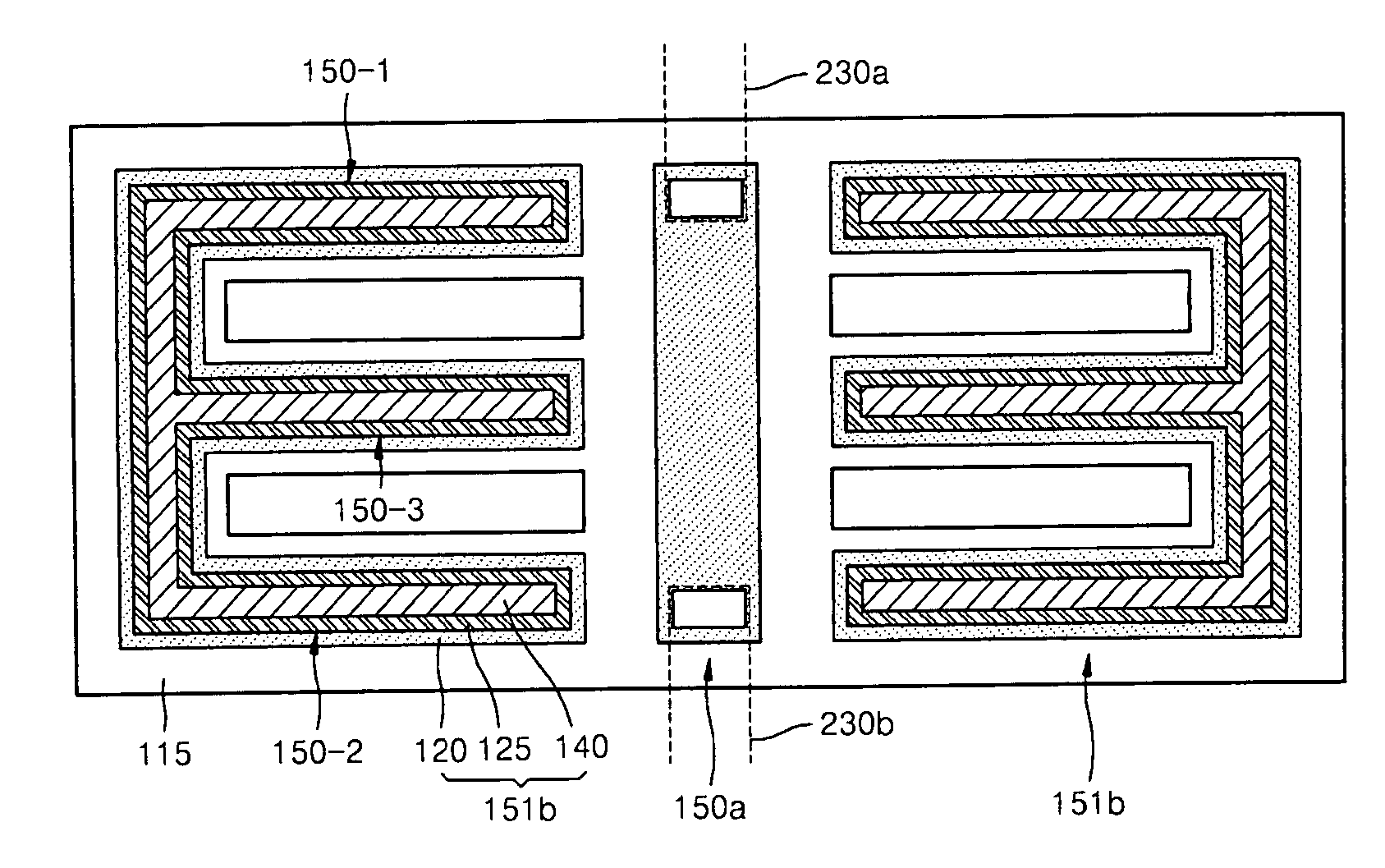
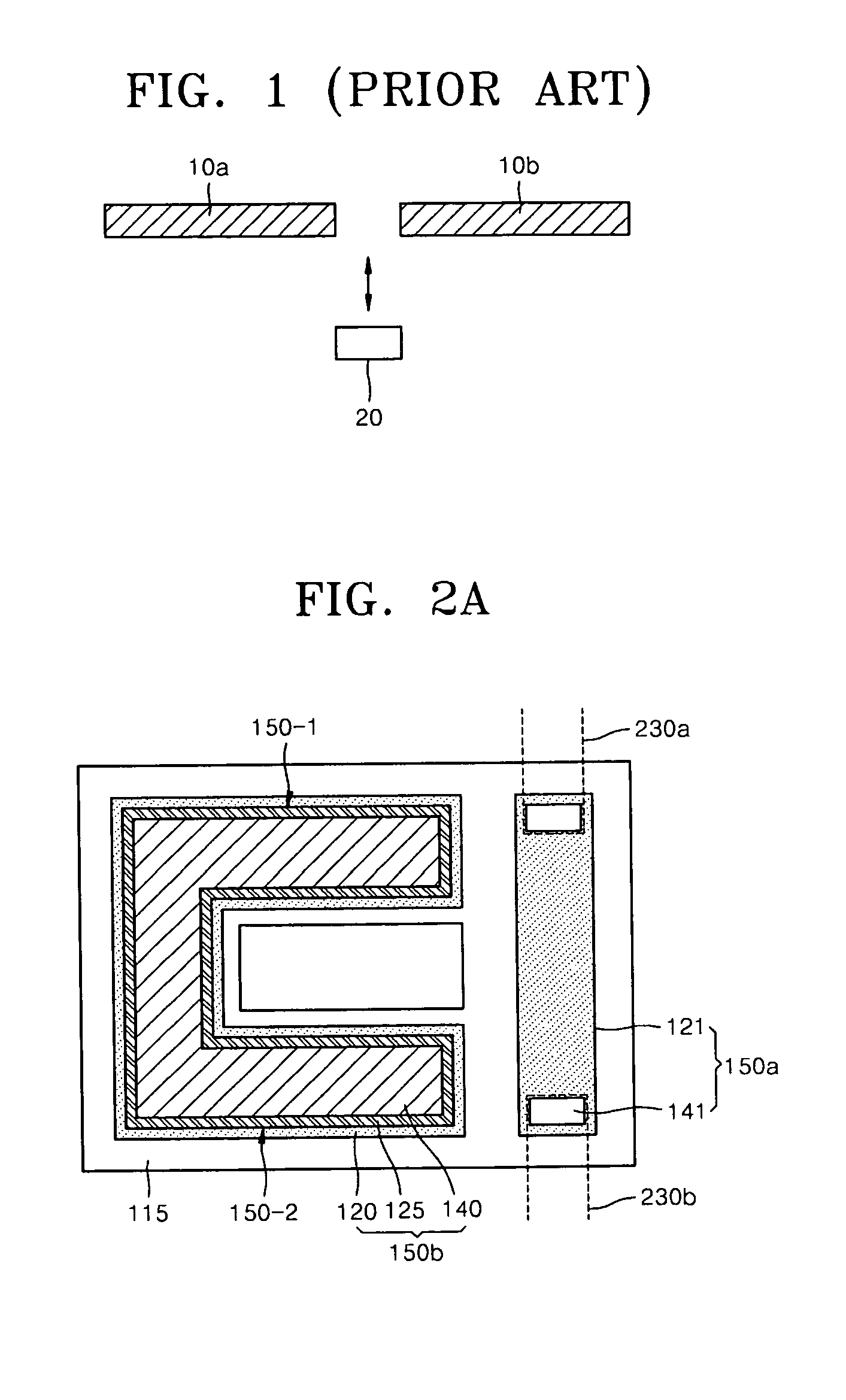
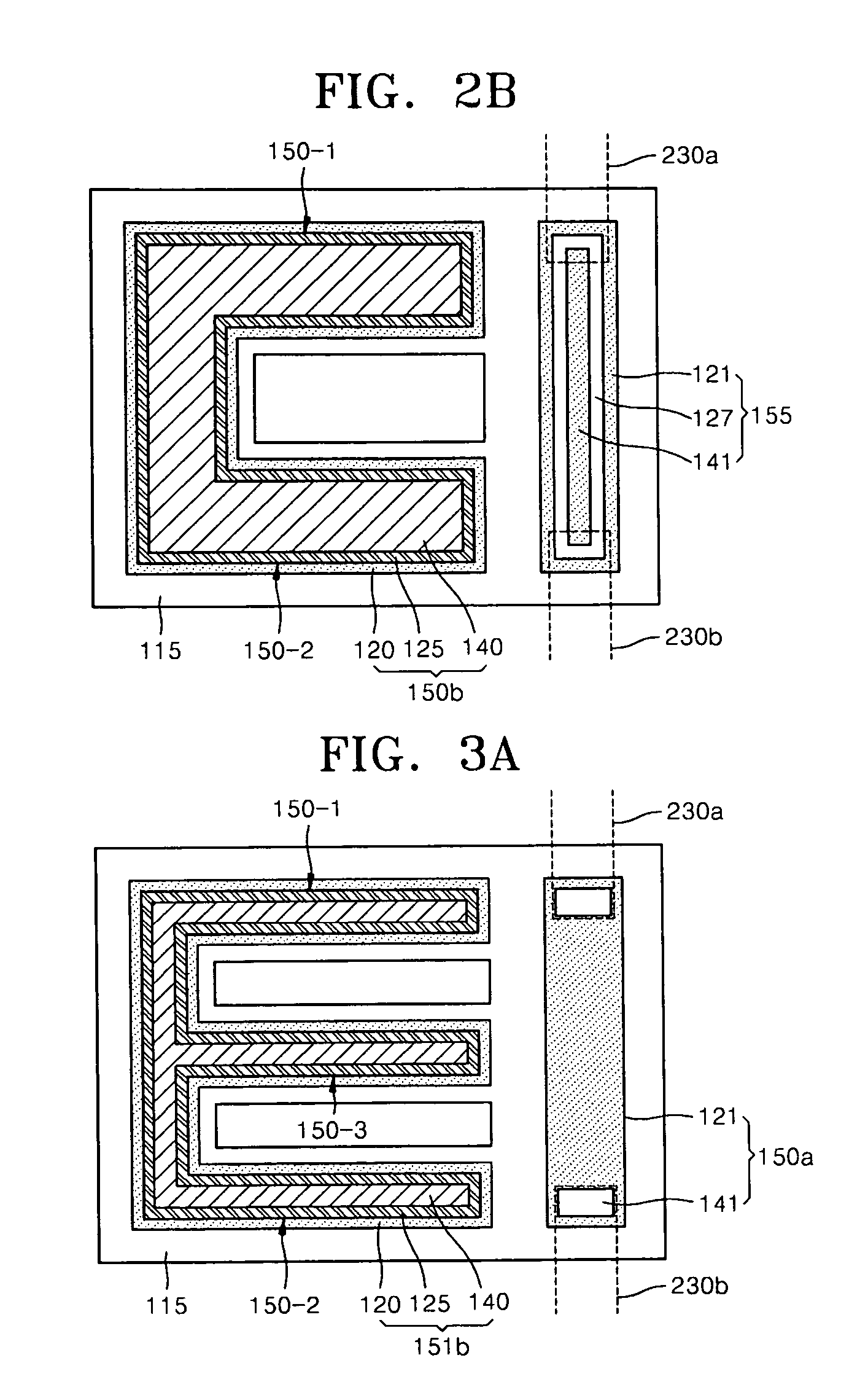
[0029]FIG. 2A is a plan view illustrating a piezoelectric MEMS switch according to an embodiment of the present invention.

[0030]Referring to FIG. 2A, a support 115 is formed on a semiconductor substrate (not shown). The support 115 may be formed of an insulating layer, e.g., a silicon nitride layer. The support 115 defines an area in which one switch will be formed. Although not shown in FIG. 2A, the semiconductor substrate includes...


PUM


Abstract

A piezoelectric micro electro-mechanical system switch (MEMS), an array of piezoelectric MEMS switches, and a method of fabricating the switch, which are capable of improving low voltage and switching characteristics while securing high signal isolation, are provided. The piezoelectric MEMS switch includes a semiconductor substrate including a groove, a support formed over the semiconductor substrate and the groove. An actuator including a piezoelectric layer is formed on the support. A switching member is formed on the support on one side of the actuator, wherein upward movement of the switching member changes by a deformation of the piezoelectric layer of the actuator. Radio frequency (RF) transfer lines are arranged at a predetermined distance on the switching member and are separated by a predetermined interval from each other. The actuator is formed to have at least two cantilevers each having one end such that the ends are connected to each other.

Description

CROSS-REFERENCE TO RELATED PATENT APPLICATION[0001]This application claims the benefit of Korean Patent Application Nos. 10-2005-0120188, filed on Dec. 8, 2005 and 10-2006-0046282, filed on May 23 in the Korean Intellectual Property Office, the disclosures of which are incorporated herein in their entirety by reference.BACKGROUND OF THE INVENTION[0002]1. Field of the Invention[0003]The present invention relates to a piezoelectric micro electro-mechanical system (MEMS) switch, an array of piezoelectric MEMS switches, and a method of fabricating the piezoelectric MEMS switch, and more particularly, to a piezoelectric MEMS switch having an actuator in a cantilever form, an array of the switches, and a method of fabricating the piezoelectric MEMS switch.[0004]2. Description of the Related Art[0005]With the rapid development of information communication, small, light and high-performance information communication systems are highly in demand. Accordingly, the development of parts for the...

Claims


Application Information

Patent Timeline
Patent Type & Authority Patents(United States)
IPC IPC(8): H01L23/48
CPCH01H57/00H01H2057/006H01L2924/0002H01L2924/00
Inventor JUNG, SUNG HAELEE, MYUNG LAEKANG, SUNG WEON
Owner ELECTRONICS & TELECOMM RES INST
Why Eureka
Try Eureka