Single axis CCD time gated ladar sensor

a single-axis, gated technology, applied in the field of single-axis ccd time gated ladar sensors, can solve the problems of time delay measurement circuitry, high-energy laser pulses, host of design and manufacturing complexities, etc., and achieve the effect of simplifying construction

Inactive Publication Date: 2010-03-30
UNITED STATES OF AMERICA THE AS REPRESENTED BY THE SEC OF THE ARMY
View PDF12 Cites 9 Cited by
  • Summary
  • Abstract
  • Description
  • Claims
  • Application Information

AI Technical Summary

Benefits of technology

[0015]Acccordingly, one object of the invention is to provide a flash ladar radar sensor of simplified construction.
[0016]Another object of the present invention is to provide a flash ladar radar sensor that is economical to manufacture.
[0017]Another object of the present invention is to provide a flash ladar sensor for a multiple pulse scanning system that can generate accurate signal information relating to an object's range, elevation and angle in real time.

Problems solved by technology

These prior art photosensitive pixel arrays require time delay measurement circuitry for each pixel of the array.
Considering the already high level of circuit integration that had been used with imaging arrays, the addition of time delay measurement circuitry on a pixel by pixel basis has led to a host of design and manufacturing complexities.
Still further, prior art flash ladar designs require very high energy laser pulses in order to flood illuminate a relatively large volume of space.
The DRS Hadland, LTD device employs the concept of shifting charge in a masked pixel for producing a two-dimensional image but cannot be used to determine the range of an object.

Method used


Image

  • Single axis CCD time gated ladar sensor
  • Single axis CCD time gated ladar sensor
  • Single axis CCD time gated ladar sensor

Examples


Embodiment Construction

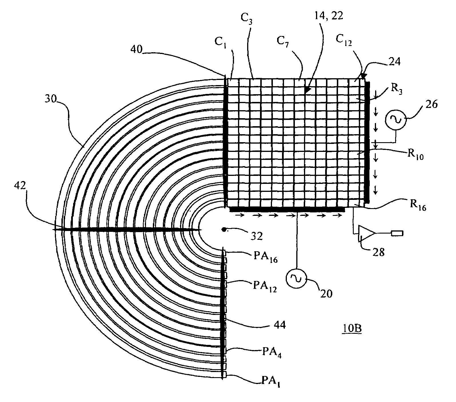
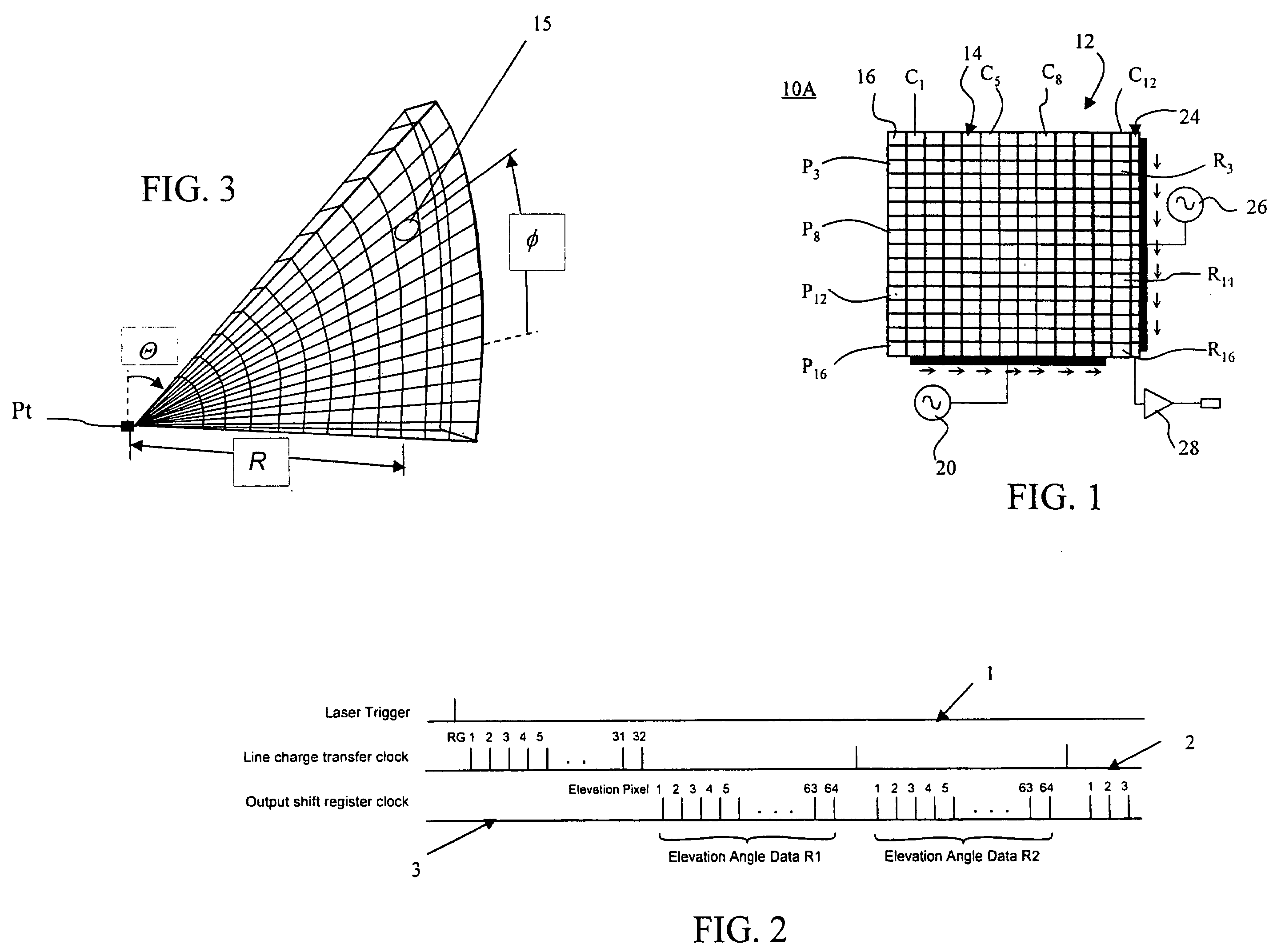
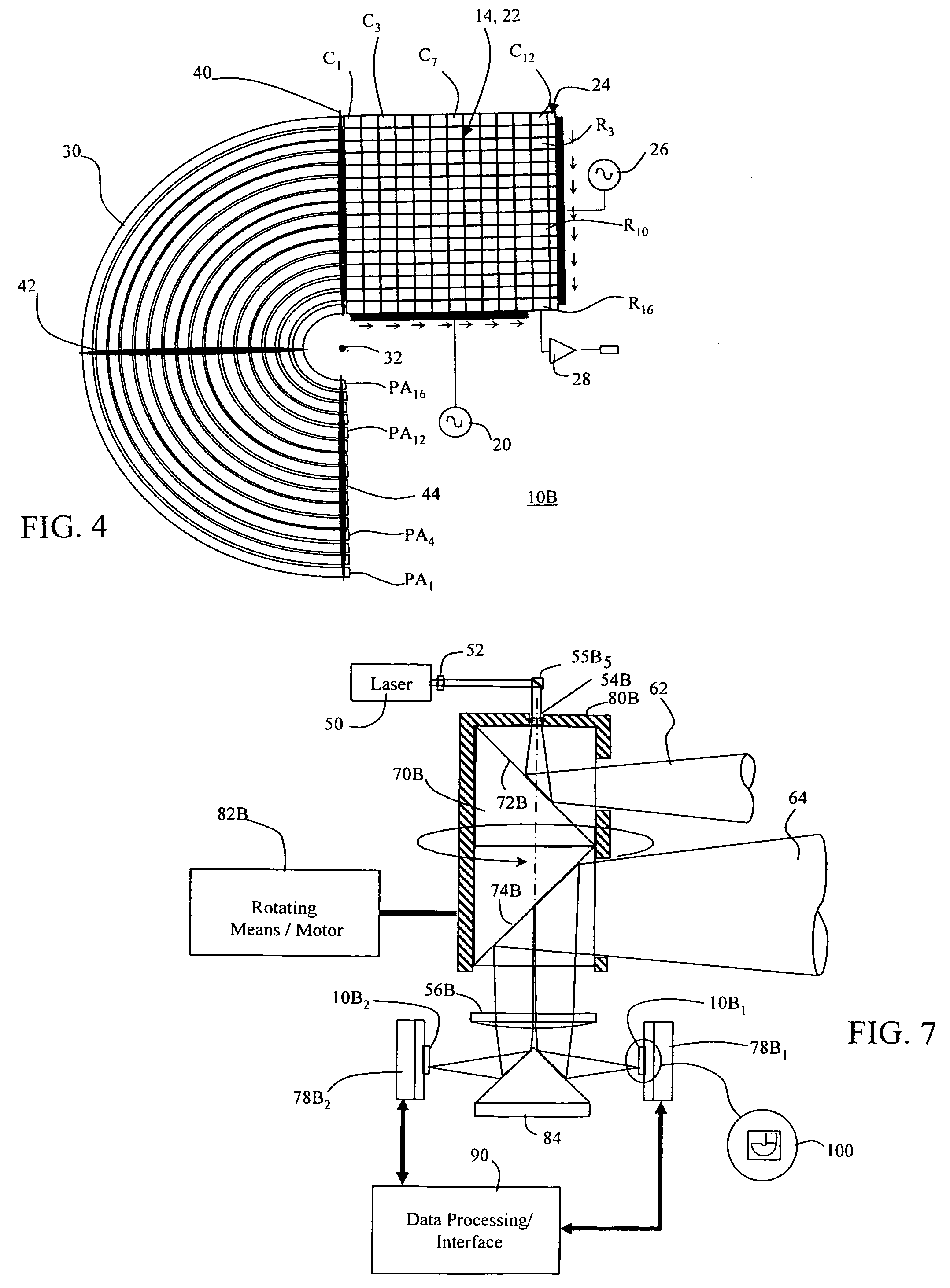
[0033]Referring now to the drawings wherein like reference numerals represent like or corresponding parts in each of the several figures, and more particularly to FIG. 1 thereof, a sensor 10A is provided with a charge storage matrix or array 12 having columns and rows of charge storage pixels 14.

[0034]In FIG. 1, the reference character C1 represents the first column of charge storage pixels, the reference character C5 represents the fifth column of charge storage pixels, the reference character C8 represents the eighth column of charge storage pixels and the reference character C12 represents the twelfth or last column of charge storage pixels. The columns of charge storage pixels may be viewed as range bins.

[0035]The third row of charge storage pixels is indicated by reference character R3, the eleventh row of charge storage pixels is indicated by reference character R11, and the last or sixteenth row of charge storage pixels is represented by reference character R16.

[0036]A photos...


PUM


Abstract

A CCD sensor device has columns and rows of masked pixels that form a charge storage matrix. A singular column of photosensitive pixels form a photosensitive region and are directly connected to the first column of the charge storage matrix. Photons received in the pixels of the photosensitive region are converted to an electrical charge over an integration period and are then shifted from the photosensitive region to the first column of the charge storage matrix. After a second integration period the integrated charge in the photosensitive region is shifted to the first column and the charges previously stored in the first column are shifted to the second column of the matrix. This process is repeated until all the columns of the storage region are full of charges at which time the charges are read out by a serial shift register.

Description

DEDICATORY CLAUSE[0001]The invention described herein may be manufactured, used and licensed by or for the U.S. Government for governmental purposes without payment of any royalties thereon.BACKGROUND OF THE INVENTION[0002]1. Field of the Invention[0003]The present invention pertains generally to devices used to measure the distance to an object. More particularly, the present invention pertains to a class of laser radar sensors known as “flash” ladar sensors.[0004]Conventional flash radar sensors use a single laser pulse to measure range to multiple spatial positions. In the present invention, the time delay of light reflected from a succession of laser pulses is measured. The laser pulses are generated at different intervals of an azimuth angle with each pulse lasting for a predetermined interval of time. By processing the signals received during each laser pulse, the range, elevation and angle of an object can be quantified in real time. The present invention uses established cha...

Claims


Application Information

Patent Timeline
Patent Type & Authority Patents(United States)
IPC IPC(8): H04N5/335G01S7/481H04N5/372
CPCG01S7/481G01S7/4863G01S17/10G01S7/4817
Inventor LAND, JAY E.
Owner UNITED STATES OF AMERICA THE AS REPRESENTED BY THE SEC OF THE ARMY
Why Eureka
Try Eureka