Liquid crystal display device with a buffer capacitor electrode disposed in a non-pixel electrode region

a liquid crystal display and buffer capacitor technology, applied in static indicating devices, instruments, non-linear optics, etc., can solve the problems of more serious display irregularities, difficult to obtain high luminance, and relative dense sticking, and achieve high display characteristics.

Active Publication Date: 2010-03-30
SHARP KK
View PDF13 Cites 34 Cited by
  • Summary
  • Abstract
  • Description
  • Claims
  • Application Information

AI Technical Summary

Benefits of technology

[0038]The invention makes it possible to provide a liquid crystal display which can achieve high display characteristics.

Problems solved by technology

As thus described, substantially no sticking occurred on the liquid crystal display which did not employ the capacitive coupling HT method, whereas the liquid crystal display employing the capacitive coupling HT method had a problem in that relatively dense sticking occurred.
Therefore, liquid crystal displays according to the related art employing the capacitive coupling HT method have a problem in that it is difficult to obtain high luminance.
The relationship between the liquid crystal capacity and the voltage ratio can result in more serious display irregularities when there is variation of the cell thickness.
That is, the liquid crystal display according to the related art employing the capacitive coupling HT method has a problem in that display irregularities are highly visible because fluctuation of the cell thickness results in a synergetic effect between variation of transmittance attributable to variation of the retardation and variation of transmittance attributable to variation of the voltage ratio.

Method used


Image

  • Liquid crystal display device with a buffer capacitor electrode disposed in a non-pixel electrode region
  • Liquid crystal display device with a buffer capacitor electrode disposed in a non-pixel electrode region
  • Liquid crystal display device with a buffer capacitor electrode disposed in a non-pixel electrode region

Examples


first embodiment

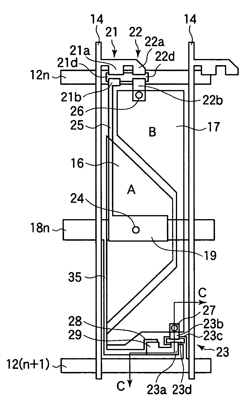
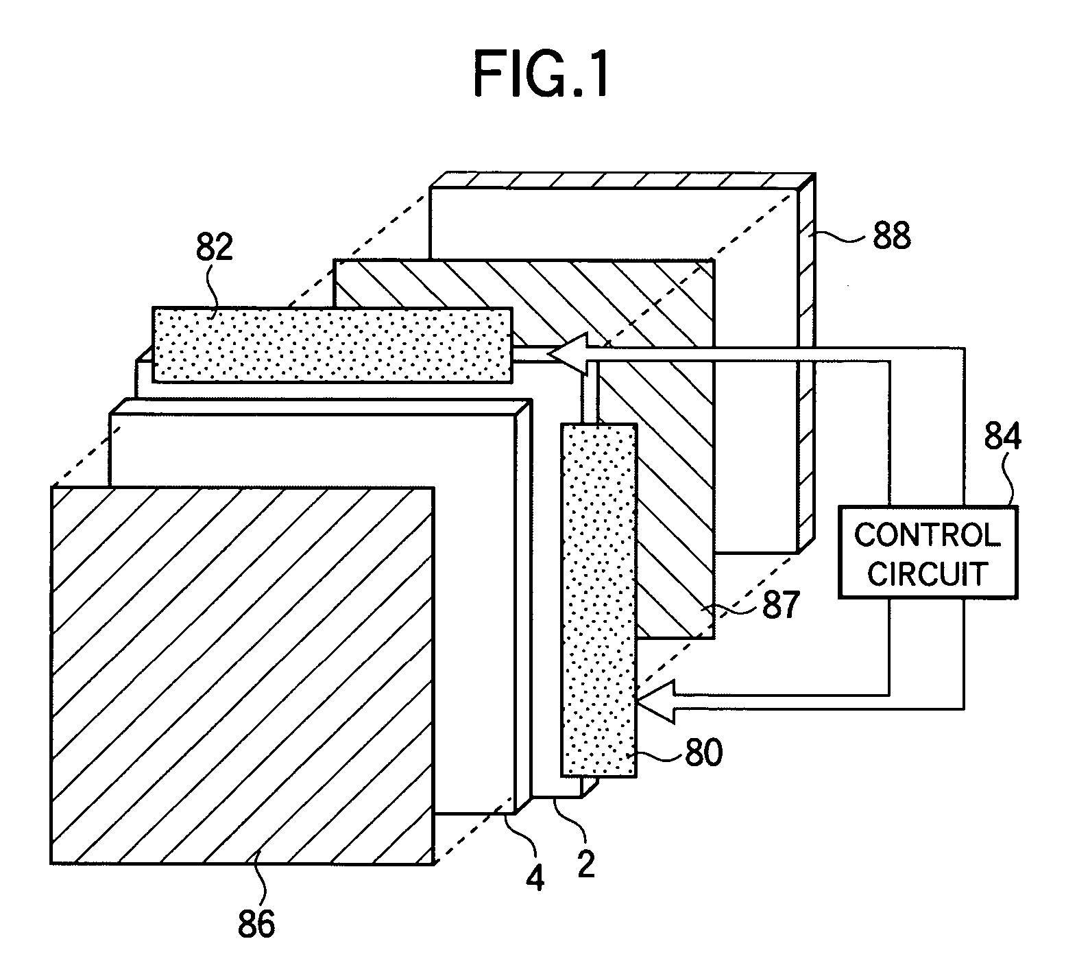
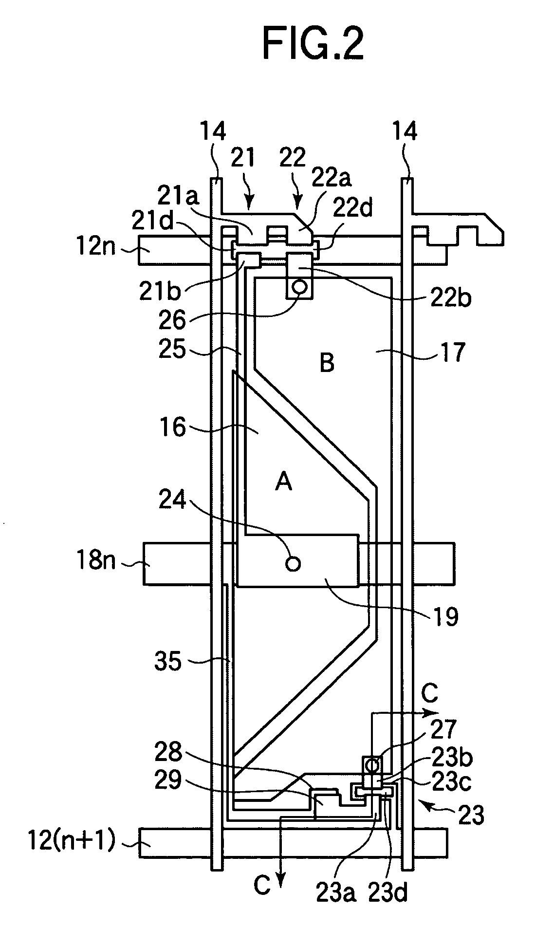
[0067]A description will now be made with reference to FIGS. 1 to 13 on a substrate for a liquid crystal display, a liquid crystal display having the substrate, and a method of driving the display according to a first embodiment of the invention. FIG. 1 shows a schematic configuration of the liquid crystal display of the present embodiment. As shown in FIG. 1, the liquid crystal display includes a TFT substrate 2 having gate bus lines and drain bus lines formed across each other with an insulation film interposed between them and a TFT and a pixel electrode formed at each pixel. The liquid crystal display also includes an opposite substrate 4 having color filters and a common electrode formed thereon and a liquid crystal 6 (not shown in FIG. 1) having, for example, negative dielectric constant anisotropy sealed between the substrates 2 and 4.

[0068]A gate bus line driving circuit 80 loaded with a driver IC for driving the plurality of gate bus lines and a drain bus line driving circu...

second embodiment

[0091]A description will now be made with reference to FIGS. 14 to 15D on a liquid crystal display according to a second embodiment of the invention. In the liquid crystal display of the first embodiment of the invention, although a relatively high light transmittance can be achieved even at a sub-pixel B, luminance may not be improved so much because of a reduction in the aperture ratio of the pixels. As shown in FIG. 9, the most significant factor reducing the aperture ratio is the TFT 23. FIG. 14 shows a configuration of the liquid crystal display of the present embodiment. As shown in FIG. 14, in the present embodiment, a TFT 23 is disposed such that it extends across a gate bus line 12(n+1) that belongs to the next pixel. As a result, the area occupied by the TFT 23 in the pixel region of interest is reduced to improve the aperture ratio of the same.

[0092]However, when the TFT 23 is disposed so as to extend across the next gate bus line 12(n+1), either drain electrode 23a or so...

third embodiment

[0095]A description will now be made with reference to FIGS. 16 and 17 on a liquid crystal display according to a third embodiment of the invention. A factor that reduces the yield of manufacture of liquid crystal displays according to the second embodiment as shown in FIG. 14 is shorting defect between the drain bus line 14 and the connection electrode 25. Since the drain bus line 14 and the connection electrode 25 are formed in the same layer and are extended a relatively long distance in proximity to each other, a shorting defect attributable to such as dust is likely to occur at a photolithographic process. When the connection electrode 25 and the pixel electrode 17 of the sub-pixel B are disposed in an overlapping relationship, a capacity formed between the connection electrode 25 and the pixel electrode 17 will decrease the voltage at the pixel electrode 16 of the sub-pixel A, which results in a reduction of the luminance of the pixel as a whole. When the interval between the ...


PUM

PropertyMeasurementUnit
polar angleaaaaaaaaaa
timeaaaaaaaaaa

Abstract

The invention relates to a substrate for a liquid crystal display, a liquid crystal display having the substrate, and a method of driving the display and provides a substrate for a liquid crystal display which allow high display characteristics to be achieved, a liquid crystal display having the substrate, and a method of driving the display.The substrate includes two TFTs having gate electrodes connected to a gate bus line and drain electrodes connected to a drain bus line, a pixel electrode connected to a source electrode, a pixel electrode connected to another source electrode and separated from the pixel electrode, another TFT having a gate electrode connected to another gate bus line and a source electrode connected to the pixel electrode, and a buffer capacitor portion having a buffer capacitor electrode connected to another drain electrode and another buffer capacitor electrode connected to a storage capacitor bus line.

Description

BACKGROUND OF THE INVENTION[0001]1. Field of the Invention[0002]The present invention relates to a substrate for a liquid crystal display used in a display section of an electronic apparatus, a liquid crystal display having the substrate, and a method of driving the display.[0003]2. Description of the Related Art[0004]Recently, liquid crystal displays have been put in use as monitoring device of television receivers and personal computers. In such applications, high viewing angle characteristics must be achieved to allow a display screen to be viewed in all directions. FIG. 20 is a graph showing transmittance characteristics relative to applied voltages (T-V characteristics) of a VA (Vertically Aligned) mode liquid crystal display. The abscissa axis represents voltages (V) applied to a liquid crystal layer, and the ordinate axis represents light transmittance. The line A indicates T-V characteristics in a direction perpendicular to the display screen (hereinafter referred to as “a s...

Claims


Application Information

Patent Timeline
Patent Type & Authority Patents(United States)
IPC IPC(8): G02F1/136G02F1/1343
CPCG02F1/134309G02F1/13624G02F1/136213G02F2001/134345G09G2300/04G02F1/134345G02F1/133G02F1/1343
Inventor UEDA, KAZUYAKAMADA, TSUYOSHINAKANISHI, YOHEIYOSHIDA, HIDEFUMITSUDA, HIDEAKISHIBASAKI, MASAKAZUTASAKA, YASUTOSHI
Owner SHARP KK
Why Eureka
Try Eureka