Optical sensor element and method for driving the same

a technology of optical sensor element and optical sensor, which is applied in the direction of basic electric elements, electrical apparatus, semiconductor devices, etc., can solve the problems of small magnitude of photocurrent and increase in process number, and achieve the effect of small output variation and large photocurrent outpu

Inactive Publication Date: 2010-04-06
KK TOSHIBA
View PDF2 Cites 5 Cited by
  • Summary
  • Abstract
  • Description
  • Claims
  • Application Information

AI Technical Summary

Problems solved by technology

However, the vertical pin structure has a problem that the number of processes increases because it cannot be formed by using the same process as that of the TFTs for driving the photodiodes.
On the other hand, the lateral pin structure has a problem that the magnitude of the photocurrent becomes small although the structure can be formed in the same process as that of TFTs for driving the photodiodes.
Furthermore, if the length of an i-region serving as a light receiving part of a photodiode in a direction sandwiched between a p-region and an n-region is lengthened, the value of the photocurrent varies among photodiodes having the same structure, resulting in another problem.

Method used


Image

  • Optical sensor element and method for driving the same
  • Optical sensor element and method for driving the same
  • Optical sensor element and method for driving the same

Examples


first embodiment

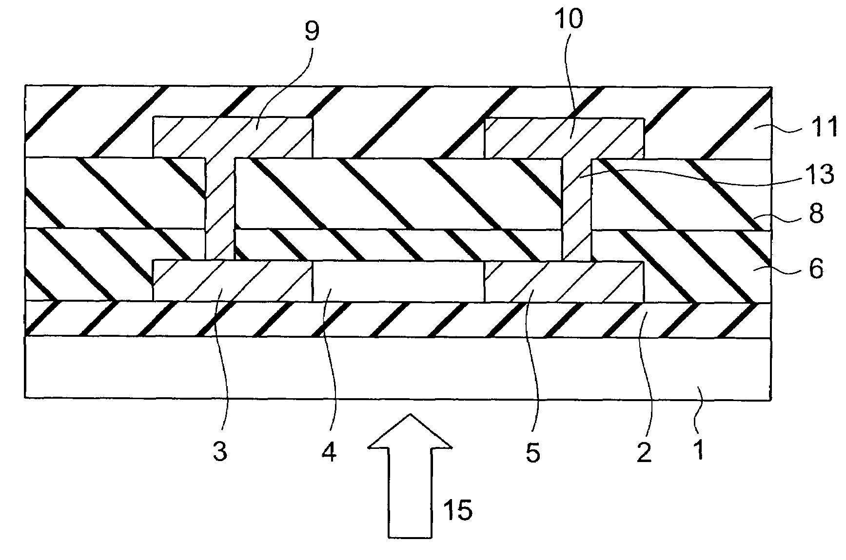
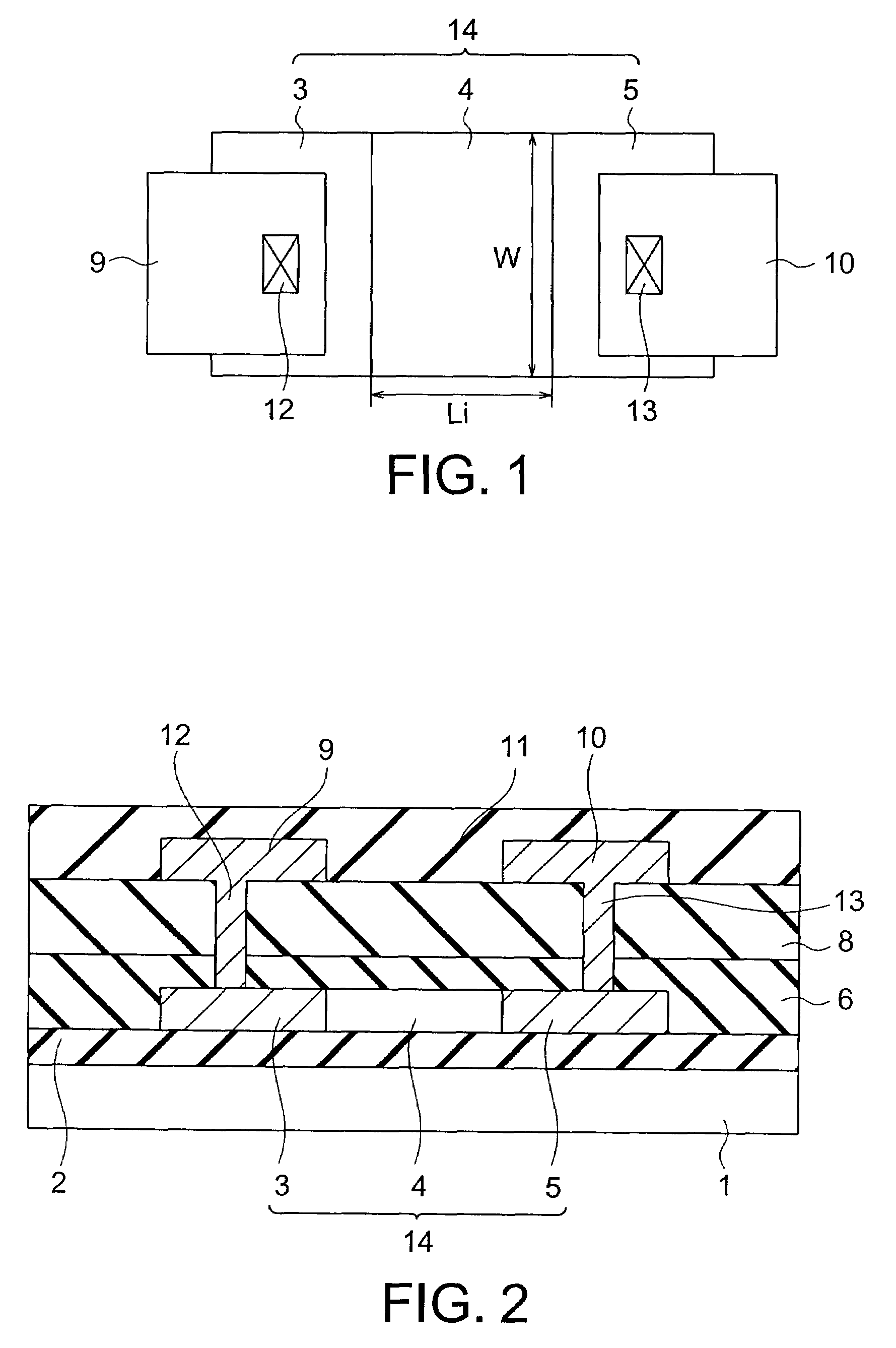
[0056]An optical sensor element according to a first embodiment of the present invention will now be described. The optical sensor element according to the present embodiment is a lateral pin structure diode. Its plan view is shown in FIG. 1 and its sectional view is shown in FIG. 2.

[0057]An undercoat layer 2 formed of silicon nitride (SiNx) or silicon oxide (SiOx) is formed on a glass substrate 1 so as to have a thickness in the range of 50 to 200 nm by using the plasma CVD (Chemical Vapor Deposition) method or the like. A polycrystalline silicon film is formed on the undercoat layer 2 so as to have a thickness in the range of approximately 50 to 100 nm. This polycrystalline silicon film includes a p+-region 3 doped with boron having a high concentration of approximately 1×1019 cm−3, an n+-region 5 doped with phosphorus having a high concentration of approximately 1×1019 cm−3, and an i-region 4 which is provided between the p+-region 3 and the n+-region 5 and which is lower in conc...

second embodiment

[0065]A second embodiment of the present invention is a TFT array. A TFT array is formed by arranging the optical sensor elements of lateral pin structure diode type according to the first embodiment and thin film transistors on a substrate in a matrix form. A TFT-LCD with optical sensors integrally formed is thus implemented.

[0066]It becomes possible to conduct operation in the irradiation light intensity-determining region and reduce the variation ξ of the photocurrent as compared with that in operation in the lifetime-determining region, by making the reverse bias voltage Vb applied at the time of photocurrent detection higher than the saturation voltage Vsat so as to satisfy the following relation.

Vsat<VbVsat  (20)

The saturation voltage Vsat varies by approximately 20% at maximum among elements. By selecting the length Li of the i-region 4 so as to satisfy the expression (20), therefore, the photodiode is made to operate in the irradiation light intensity-determining region w...

third embodiment

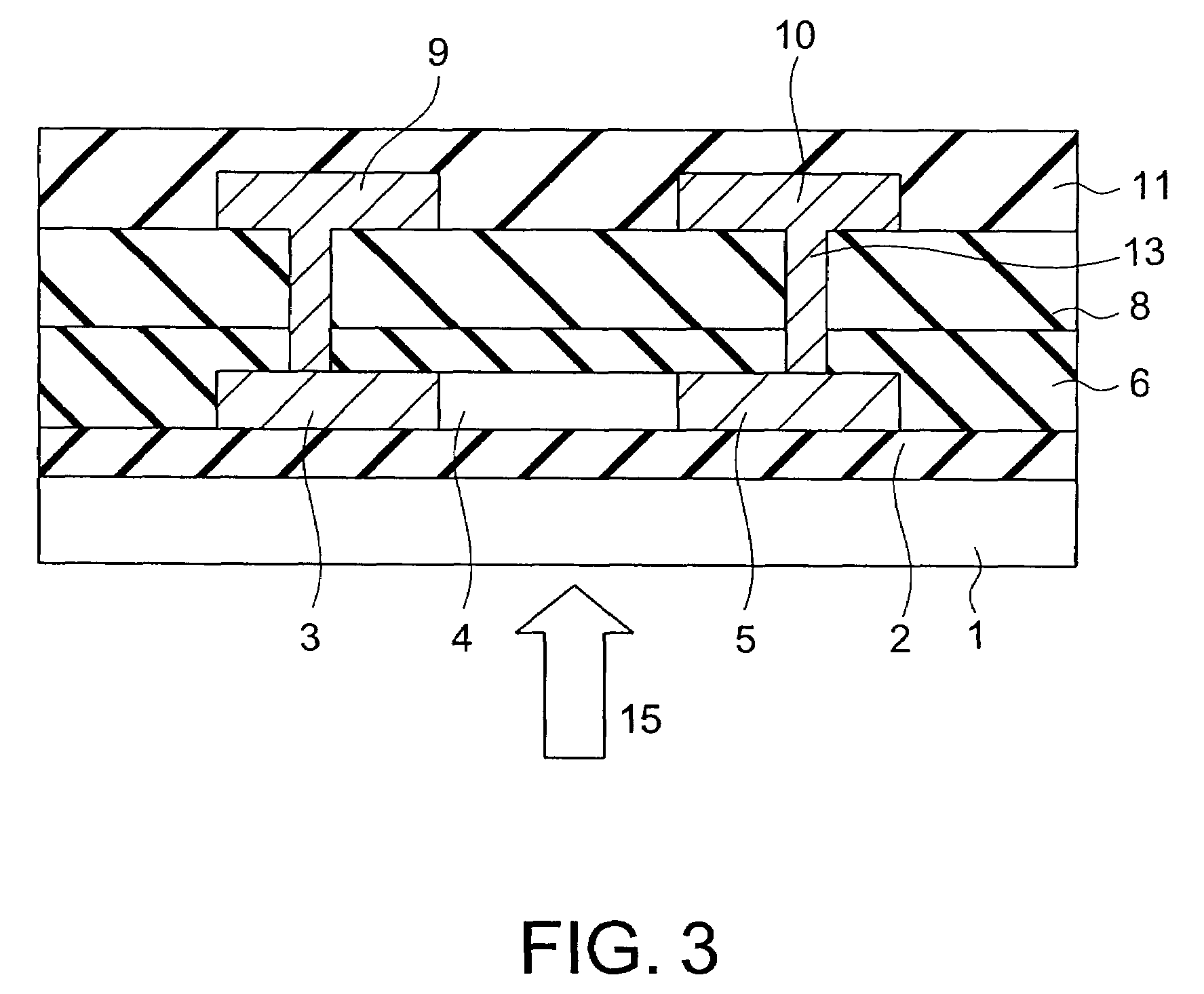
[0067]An optical sensor element of lateral pin structure diode type according to a third embodiment of the present invention will now be described. A plan view and a sectional view of the optical sensor element (photodiode) according to the present embodiment are shown in FIGS. 6 and 7, respectively.

[0068]The optical sensor element according to the present embodiment has a configuration obtained from the optical sensor element according to the first embodiment shown in FIGS. 1 and 2 by providing a gate electrode 7 on the silicon oxide film (gate insulation film) 6 so as to cover a partial region of the i-region 4. In the present embodiment, the partial region of the i-region 4 is provided on the anode electrode 9 side, and the partial region of the i-region 4 is shorter in length than the length Li of the i-region 4, but has the same width W as that of the i-region 4. By the way, the gate electrode 7 is covered by the silicon oxide film 8.

[0069]In the same way as the first embodimen...


PUM


Abstract

An optical sensor element includes: an n-type semiconductor region formed on a substrate; an i-type semiconductor region which is formed on the substrate between the p-type semiconductor region and the n-type semiconductor region and which is lower in impurity concentration than the p-type semiconductor region and the n-type semiconductor region; an anode electrode formed on the insulation film and connected to the p-type semiconductor region; and a cathode electrode formed on the insulation film and connected to the n-type semiconductor region. A reverse bias voltage Vb is applied when detecting the photocurrent, the reverse bias voltage Vb satisfying a following relation.V1<Vb<Vsat

Description

CROSS-REFERENCE TO RELATED APPLICATION[0001]This application is based upon and claims the benefit of priority from prior Japanese Patent Application No. 2007-58798 filed on Mar. 8, 2007 in Japan, the entire contents of which are incorporated herein by reference.BACKGROUND OF THE INVENTION[0002]1. Field of the Invention[0003]The present invention relates to an optical sensor element of lateral pin structure diode type, and its drive method.[0004]2. Related Art[0005]In recent years, photodetection elements (such as photodiodes) using polycrystalline silicon or amorphous silicon formed as a film on a substrate by using the CVD method have been developed vigorously. A planar type illuminance detector is implemented by arranging photodiodes on a substrate. These photodiodes can be formed on a glass substrate or the like by diverting the technique of the thin film transistor (TFT) array used in, for example, liquid crystal displays.[0006]In the typical conventional photodiodes, a reverse ...

Claims


Application Information

Patent Timeline
Patent Type & Authority Patents(United States)
IPC IPC(8): H01L31/075H01L31/10
CPCH01L31/1055H01L31/035272Y02E10/548
Inventor HARA, YUJIROKINNO, AKIRAHIOKI, TSUYOSHIAMEMIYA, ISAOUCHIKOGA, SHUICHI
Owner KK TOSHIBA
Why Eureka
Try Eureka