Evaluation method and manufacturing method of semiconductor device

a technology for semiconductor devices and manufacturing methods, applied in semiconductor/solid-state device testing/measurement, instruments, basic electric elements, etc., can solve the problems of inability to detect leakage failure, inability to accurately measure, and difficulty in detecting leakage failures. , to achieve the effect of improving the reliability of semiconductor devices, accurate measurement, and reducing the percent of defectives

Inactive Publication Date: 2006-02-02
HITACHI LTD +1
View PDF4 Cites 73 Cited by
  • Summary
  • Abstract
  • Description
  • Claims
  • Application Information

AI Technical Summary

Benefits of technology

[0013] An object of the present invention is to provide a method for evaluating leakage property of a semiconductor device capable of solving the problems described above. In this method, the leakage property of a pn junction which forms a semiconductor device on a wafer can be accurately measured at a practical speed in a noncontact manner in the early stage of the semiconductor manufacturing process, the magnitude of leakage current and its distribution and the relation between the leakage current and the leakage occurrence position are clarified to grasp the problems in the course of the process, and thus, measures for the problems can be quickly taken for the manufacturing process. In addition, another object of the present invention is to provide the method for quickly inspecting a wafer in the course of the process in a noncontact manner so as to grasp the distribution of the leakage failure and the leakage current and estimate the yield of the samples and manufacturing process in an early stage of the manufacture.
[0014] Further, another object of the present invention is to provide a method and system for evaluating the leakage property and a manufacturing method of a semiconductor device, in which the technologies described above are applied to the semiconductor device and other minute patterns formed through various types of processes so as to perform the optimization of the process for forming the junction and the management of the process, and the results thereof are reflected on the manufacturing conditions to improve the reliability of the semiconductor device and contribute to the reduction of the percent defective.

Problems solved by technology

Therefore, even if the failure occurs in this stage, the failure cannot be detected until the wafer is completed and the electric test is executed, and it takes a considerable amount of time from the occurrence of the failure to the implementation of the measures for the failure.
Also, in the development stage of the semiconductor, the failure in the formation of the minute patterns frequently occurs in each process.
When such a failure occurs, the leakage failure cannot be detected even by-the electric test.
More specifically, in the conventional case, only after the development of the forming process of a minute pattern is finished and it becomes possible to prevent the occurrence of the failure in this process, the failure in the early stage of the manufacturing process is detected in the evaluation using the completed wafer.
Also, in the inspecting method in which the electron beam is irradiated to transistors to measure the leakage amount based on the absorption current, since the absorption current is weak, it takes a significant time to inspect one area.
Therefore, it is not suitable for evaluating the leakage property of a wide area of the wafer in a practical time.
Also, even in the method in which the electron beam is irradiated to the wafer which is being processed and the electrical properties of the semiconductor device are inspected based on the voltage contrast, the failure of the junction leakage cannot be inspected.
However, the technology for securing the accuracy in this translation method into the leakage current is not disclosed in the conventional technologies.

Method used


Image

  • Evaluation method and manufacturing method of semiconductor device
  • Evaluation method and manufacturing method of semiconductor device
  • Evaluation method and manufacturing method of semiconductor device

Examples


first embodiment

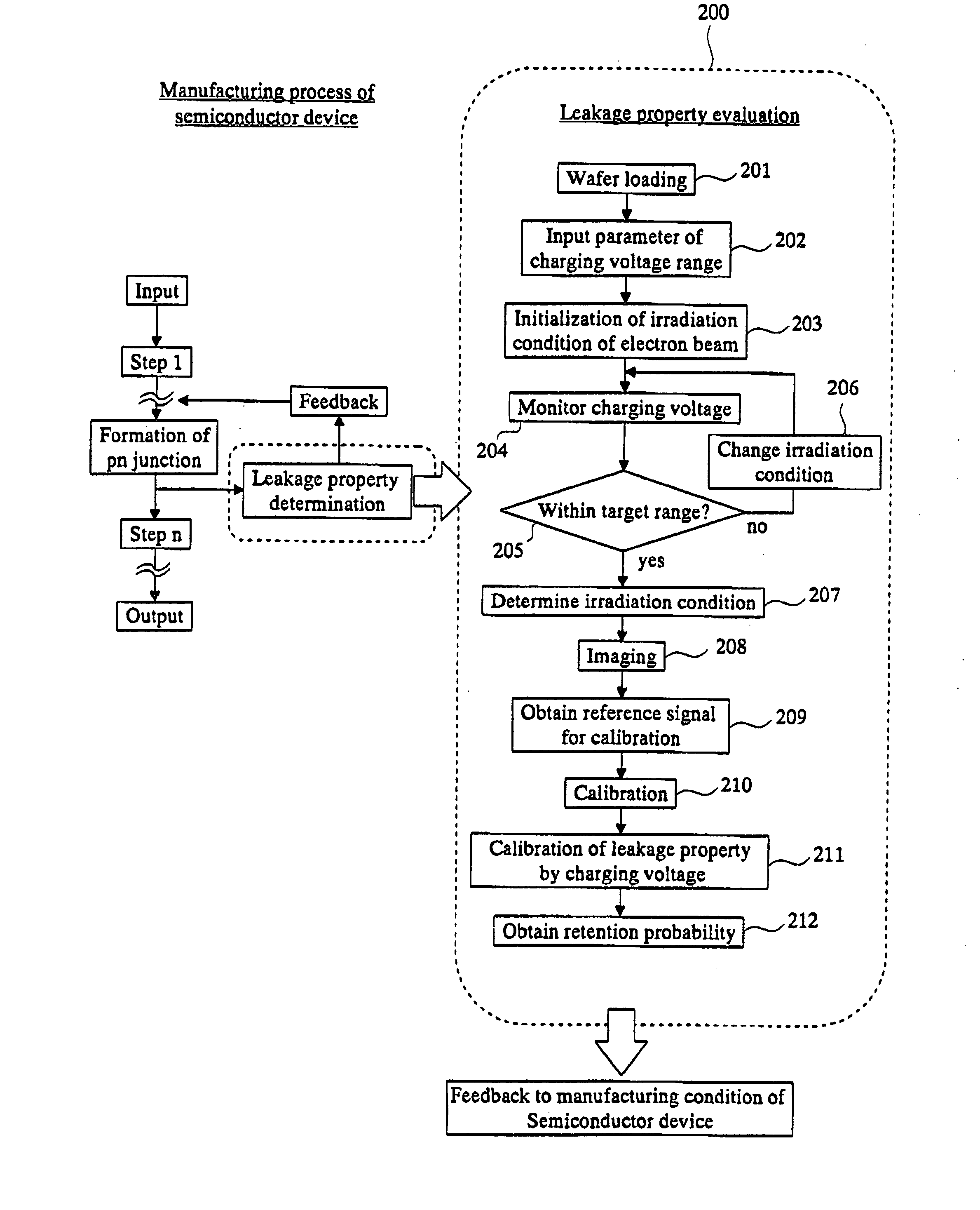
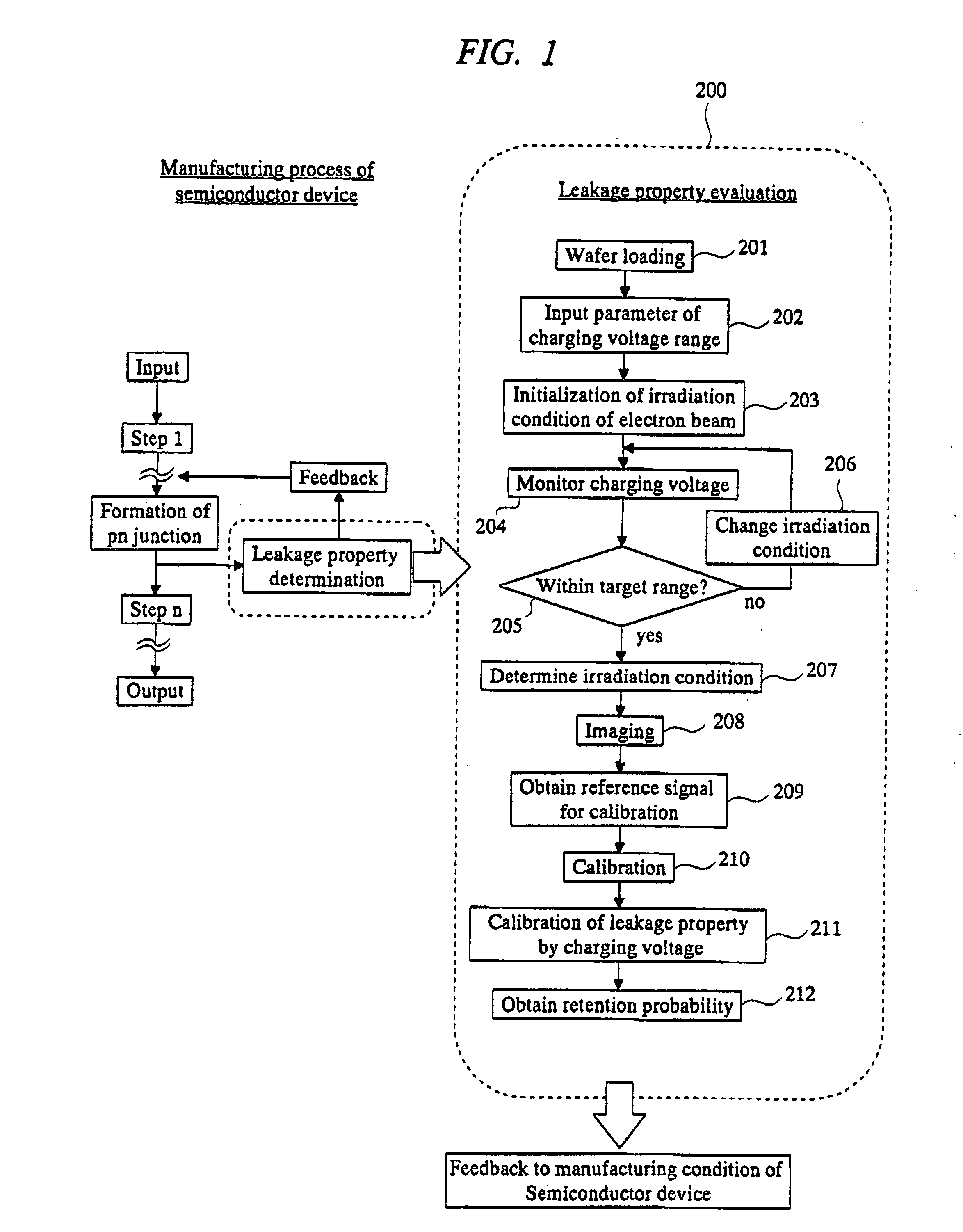
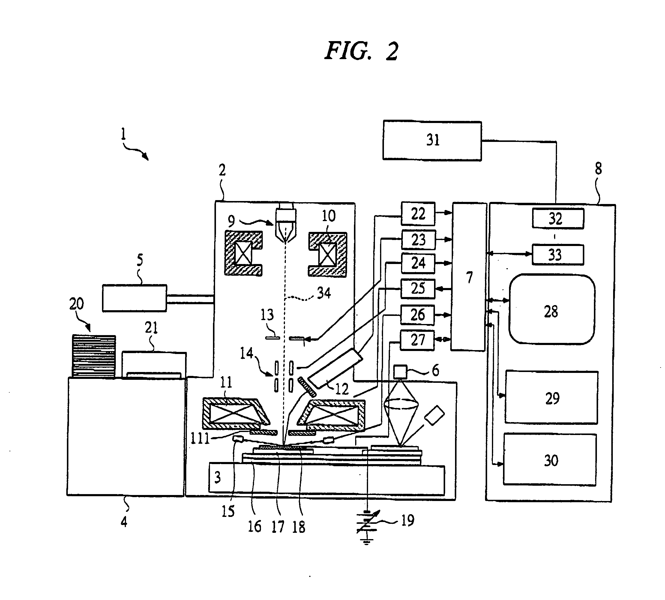
[0042] In this embodiment, the evaluation method of leakage property and the evaluation system are provided, in which the reverse bias current property (leakage property) is evaluated while monitoring the charging state on the surface of the plug connected to the device in the wafer on which the semiconductor devices in the course of the manufacturing process are fabricated.

[0043] First, the flow of the evaluation method of the leakage property of a semiconductor device according to this embodiment will be described in brief. FIG. 1 shows the flow of the method. After inputting a wafer into the semiconductor manufacturing apparatus, the process is started from the step 1. When the step of forming the pn junction is finished, the wafer on which the plugs are exposed is taken out, and the main evaluation 200 is started. First, as a step 1 (201), the wafer on which the pn junction has been formed is loaded (carried) in the evaluation system. Then, as a step 2 (202), a desired charging...

second embodiment

[0093] Next, as the second embodiment, the manufacturing method of a semiconductor device will be described, in which the evaluation method shown in the first embodiment is applied to the manufacturing process of a semiconductor device to give the feedback to the semiconductor manufacturing conditions in an early stage. By applying the evaluation method in the course of the manufacturing process, it becomes possible to know the leakage current distribution of a DRAM, the leakage current of the normal bits which form the main profile and that of the abnormal bits which form the tail profile, and the number and ratio of the abnormal bits in an early stage. Consequently, the process conditions capable of reducing the leakage current and the number and ratio of the abnormal bits can be determined in the step of forming a junction in a shorter time than that of the conventional technology.

[0094] In the development of the DRAM, the evaluation of the reverse bias current in the pn junctio...

third embodiment

[0098] The case where the present invention is applied to the wafer in the manufacturing line processed through the steps shown in FIG. 17 to FIG. 20 in the manufacturing process of a stack-type DRAM to give the feedback to the adjustment conditions of the processing apparatus will be described below.

[0099] As shown in FIG. 17, a p type substrate 51 with a specific resistance of about 10 Ωcm is prepared, and shallow trenches 52 are formed in the main surface of the substrate 51. Thereafter, a silicon oxide film 53 is formed by the thermal oxidation of the substrate 51. Then, a silicon oxide film is deposited and is polished by the CMP (Chemical Mechanical Polishing) to leave the silicon oxide film only in the shallow trenches 52, thereby forming the isolation areas 54. Next, a n type impurity, for example, phosphorus (P) is ion-implanted into the area (A area: memory array) of the substrate 51 on which the memory cell is to be formed, thereby forming the deep n type well 55. Also, ...


PUM


Abstract

The electron beam is irradiated several times at predetermined intervals to the wafer surface on which the plugs are exposed in the course of the manufacturing process so that the pn junction is in the reverse bias state. Then, the irradiation conditions of the electron beam are changed while monitoring the charging voltage on the plug surface, and the secondary electron signals of the circuit pattern are obtained under the irradiation conditions that the charging is within a desired range, thereby evaluating the leakage property. Since the charging voltage of the pn junction is relaxed depending on the magnitude of the leakage current during the interval, the leakage property is evaluated based on the luminance signals of the voltage contrast image. By measuring the charging voltage and setting it within a desired range, the evaluation result reflects the state in the actual operation. Therefore, the accuracy is enhanced.

Description

CROSS-REFERENCE TO RELATED APPLICATION [0001] The present application claims priority from Japanese Patent Application No. JP2004-215183 filed on Jul. 23, 2004, the content of which is hereby incorporated by reference into this application. TECHNICAL FIELD OF THE INVENTION [0002] The present invention relates to a technology for evaluating electrical properties of a semiconductor device having a pn junction portion. More particularly, the present invention relates to a technology for the nondestructive and noncontact evaluation of electrical properties of a pn junction portion formed on a semiconductor wafer in the course of the manufacturing process of a semiconductor device. BACKGROUND OF THE INVENTION [0003] The conventional semiconductor device has a pn junction formed therein. In general, the pn junction is formed under the condition capable of reducing junction leakage. However, the pn junction with high leakage is formed only occasionally due to the failure in the manufacturi...

Claims


Application Information

Patent Timeline
Patent Type & Authority Applications(United States)
IPC IPC(8): H01L23/58H01L29/00G01R31/305
CPCG01R31/2653H01L22/14H01L2924/0002H01L2924/00
Inventor TAKAFUJI, ATSUKONOZOE, MARIOYU, KIYONORI
Owner HITACHI LTD
Why Eureka
Try Eureka