Light-emitting semiconductor component comprising a protective diode

Active Publication Date: 2010-04-06
OSRAM OLED
View PDF16 Cites 10 Cited by
  • Summary
  • Abstract
  • Description
  • Claims
  • Application Information

AI Technical Summary

Benefits of technology

[0007]One object of the present invention is to provide a light-emitting semiconductor component which is distinguished by an improved protecti

Problems solved by technology

Such ESD voltage pulses can impair the operation o

Method used


Image

  • Light-emitting semiconductor component comprising a protective diode
  • Light-emitting semiconductor component comprising a protective diode

Examples


Example

DETAILED DESCRIPTION OF THE DRAWINGS

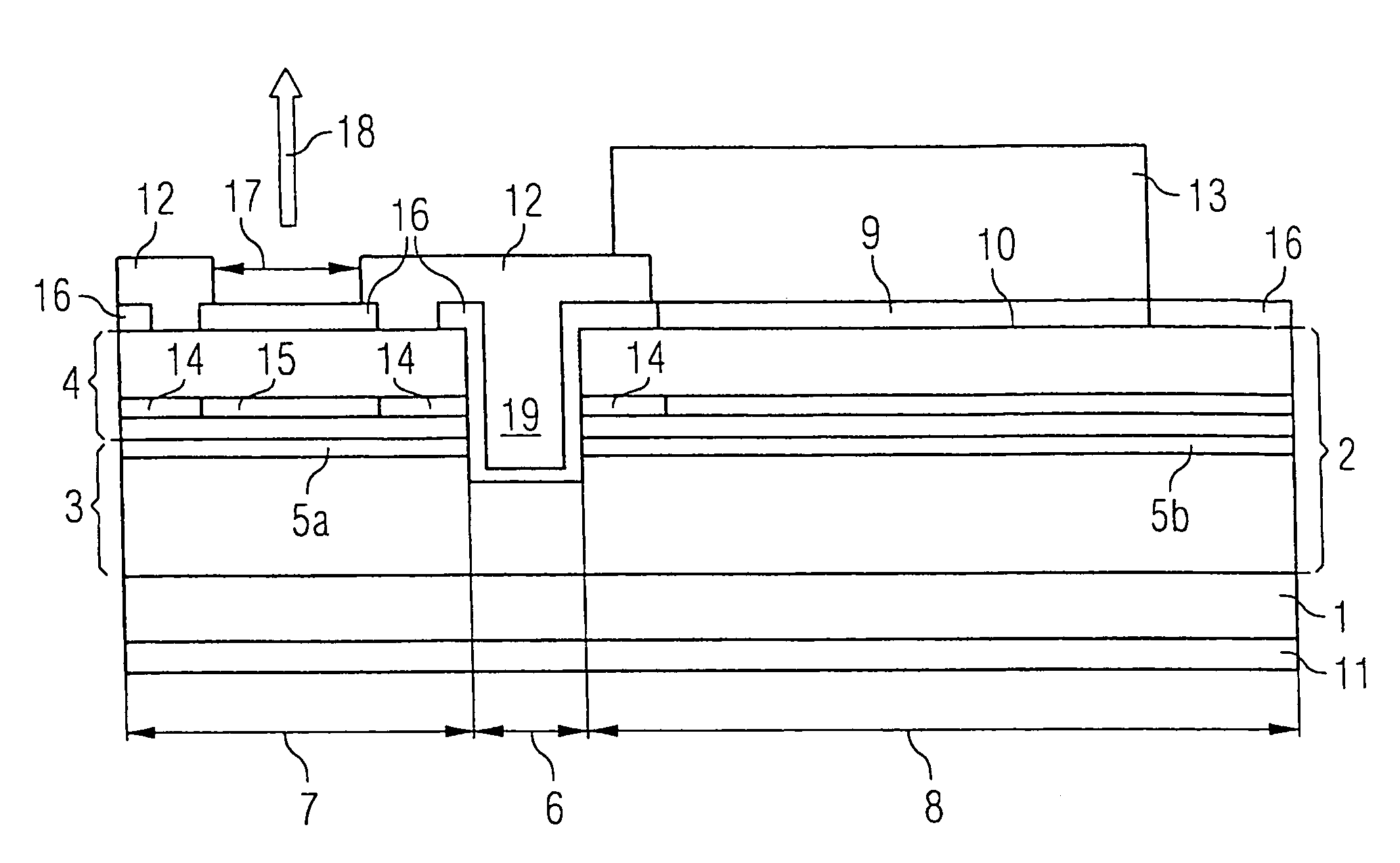
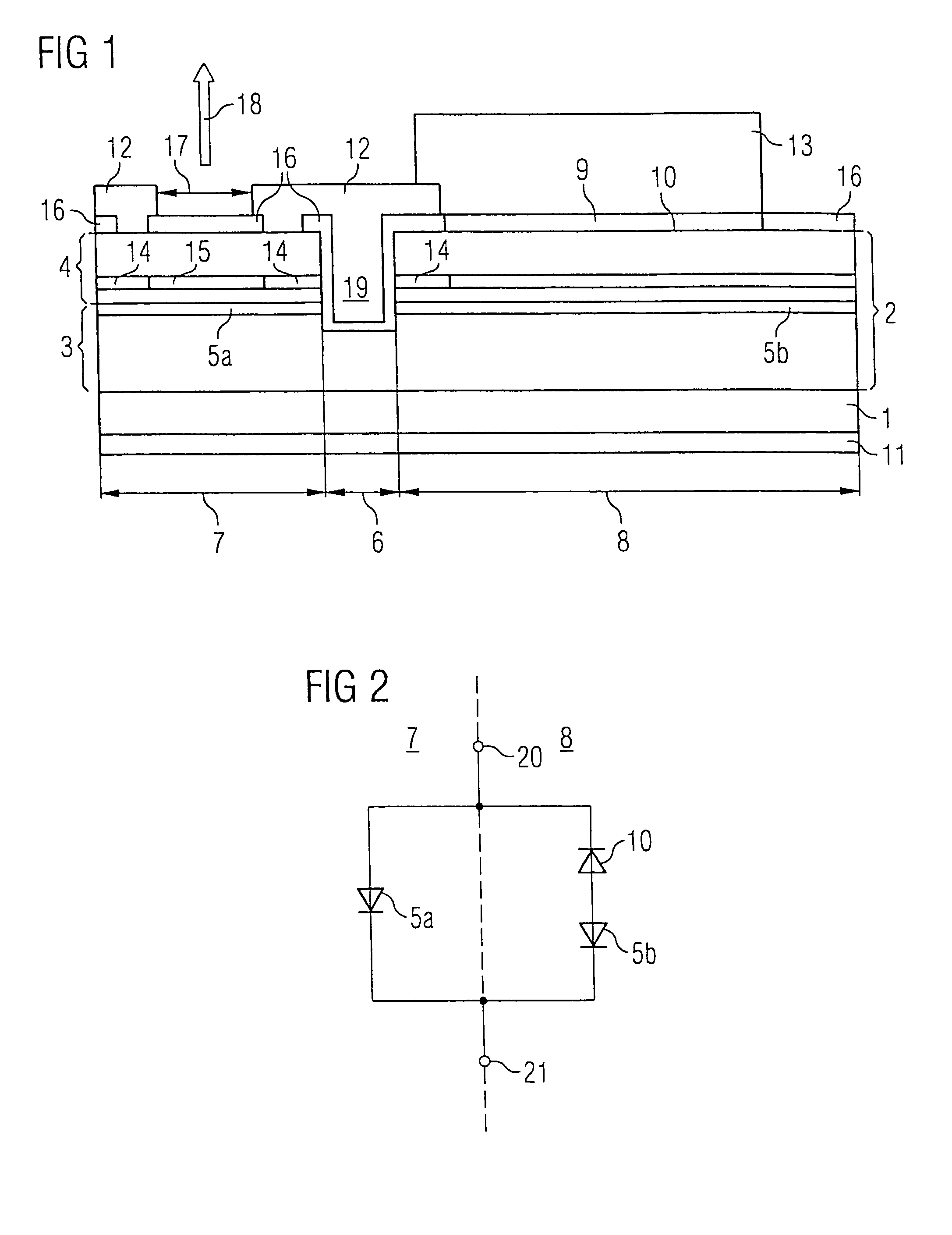
[0022]The light-emitting semiconductor component shown in FIG. 1 is a vertical cavity surface emitting laser (VCSEL). The VCSEL contains a substrate 1 to which is applied a sequence of semiconductor layers 2. The sequence of semiconductor layers 2 contains an area of n-doped layers 3 and an area of p-doped semiconductor layers 4 between which a first pn junction 5a, 5b is formed. The pn junction 5a, 5b is subdivided into a light-emitting section 7 and a protective-diode section 8 by an insulating section 6. The area of the first pn junction 5b in the protective-diode section 8 is larger, preferably larger by more than a factor of 100, than the area of the first pn junction 5a in the light-emitting section 7.

[0023]The pn junction 5a in the light-emitting section 7 represents the active zone of the VCSEL. The area of n-doped semiconductor layers 3 and the area of p-doped semiconductor layers 4 contain Bragg reflectors which in each case contain a mu...


PUM


Abstract

A light-emitting semiconductor component which contains a sequence of semiconductor layers (2) with an area of p-doped semiconductor layers (4) and n-doped semiconductor layers (3) between which a first pn junction (5a, 5b) is formed. The pn junction (5a, 5b) is subdivided into a light-emitting section (7) and a protective-diode section (8) in a lateral direction by means of an insulating section (6). An n-doped layer (9), which forms a second pn junction (10) which acts as a protective diode along with the p-doped area (4), is applied to the p-doped area (4) in the area of the protective-diode section (8), the first pn junction (5b) in the protective-diode section (8) having a larger area than the first pn junction (5a) in the light-emitting section (7). The protective-diode section (8) protects the light-emitting semiconductor component from voltage pulses due to electrostatic discharges (ESD).

Description

RELATED APPLICATIONS[0001]This is a U.S. national stage of application No. PCT / DE2004 / 002384, filed on 26 Oct. 2004.[0002]This patent application claims the priority of German patent application nos. 103 56 283.4 and 10 2004 005269.7 filed Nov. 28, 2003 and Feb. 3, 2004 respectively, the disclosure content of which is hereby incorporated by reference.FIELD OF THE INVENTION[0003]The invention relates to a light-emitting semiconductor component wherein the area of the p-doped semiconductor layers is provided in the protective-diode section on the side facing away from the first pn junction with an n-doped semiconductor layer which forms a second pn junction with the area of p-doped semiconductor layers in the protective-diode section and is electrically conductively connected to the area of p-doped semiconductor layers in the light-emitting section, and wherein the first pn junction has a larger area in the protective-diode section than in the light-emitting section.BACKGROUND OF THE ...

Claims


Application Information

Patent Timeline
IPC IPC(8): H01S5/183H01S5/125H01L23/62H01L27/15H01L33/00H01S5/026H01S5/042H01S5/068H01S5/32H01S5/40
CPCH01L27/15H01S5/0261H01S5/06825H01S5/042H01S5/40H01S5/18311H01S5/18313
Inventor ALBRECHT, TONYBRICK, PETERPHILIPPENS, MARCPLAINE, GLENN-YVES
Owner OSRAM OLED
Why Eureka
Try Eureka