Chemical vapor deposition plasma reactor having plural ion shower grids

a plasma reactor and plasma technology, applied in the direction of vacuum evaporation coating, chemical vapor deposition coating, coating, etc., can solve the problems of slow deposition rate, low wafer throughput, and unsuitable sacvd process for devices having feature sizes

Active Publication Date: 2010-04-13
APPLIED MATERIALS INC
View PDF258 Cites 181 Cited by
  • Summary
  • Abstract
  • Description
  • Claims
  • Application Information

AI Technical Summary

Problems solved by technology

Although the wafer temperature is elevated during the deposition to about 500° C., the deposited coating must be annealed at about 700°-900° C. The SACVD process is unsuitable for use on devices having feature sizes 65 nanometers or smaller, and particularly for filling HAR openings in such small devices.
First, the deposition rate is slow and the wafer throughput is low.
Secondly, this process requires a wafer anneal step, which adds to the production cost of each wafer.
Also, the high process temperature and time, and the high (900° C.) anneal temperature required in the SACVD process causes small features (such as doped sources and drains) to diffuse over a significant distance for some applications.
Such thermal induced diffusion may cause the source-to-drain channel length to shrink under a permissible threshold below which device failure can occur.
This makes its impossible to completely fill the bottom of a 65 nanometer HAR opening before the top of the opening is pinched off due to accumulation along the vertical side wall.
This leaves a void inside the opening, which is unacceptable.
A further disadvantage of the SACVD process is that it is relatively slow, requiring that the semiconductor wafer be maintained at the elevated (500° C.) temperature during deposition for a relatively long time, thereby limiting productivity and increasing the thermal diffusion of 65 nanometer features on the wafer.
As a result, when the PECVD process is used for 65 nanometer devices, deposition near the top of the side walls of HAR openings pinches off the openings before they can be filled from the bottom, leaving voids in the openings.
The problem is that the sputtering efficiency of the low density plasma employed in the PECVD process is poor.
This is due to the relatively low plasma ion density (obtained at the low voltage of the plasma source) and because the chamber pressure (5-15 Torr) is too high for efficient sputtering.
As a result, sputtering of the top edges of the HAR openings does not always prevent the pinch-off problem.
Therefore, the PECVD process is not suitable for filling HAR openings in small (e.g., 65 nanometer) devices.
As a result, at 65 nanometers, the HDPCVD process fails because of pinch-off of HAR openings before they can be completely filled from the bottom.
In summary, the advance in semiconductor technology toward 65 nanometer feature sizes is frustrated because of a lack of a reliable chemical vapor deposition process capable of completely filling HAR openings.

Method used


Image

  • Chemical vapor deposition plasma reactor having plural ion shower grids
  • Chemical vapor deposition plasma reactor having plural ion shower grids
  • Chemical vapor deposition plasma reactor having plural ion shower grids

Examples


second embodiment

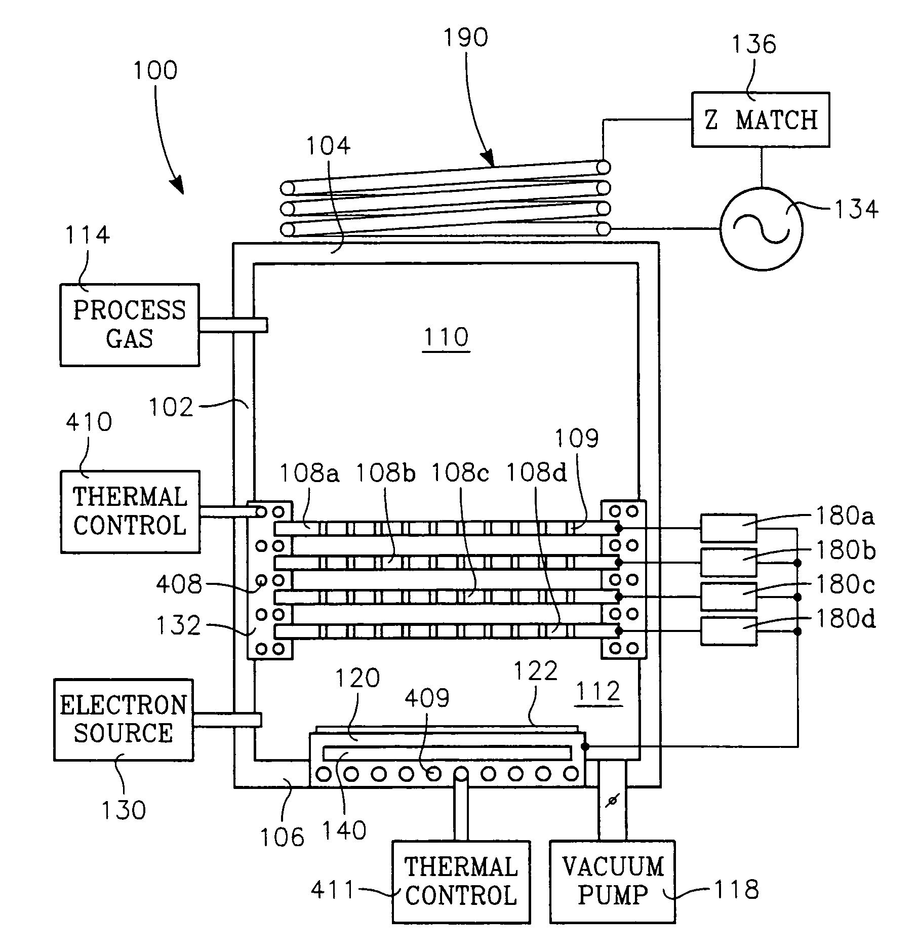
[0048]In a second embodiment, there are multiple parallel grids whose holes are in mutual vertical alignment, each grid being driven by a separate or independent voltage, these voltages being configured to provide a progressive transition from the plasma potential (at the top-most grid) to the highest grid potential (at the bottom grid).

third embodiment

[0049]In a third embodiment, the independent voltages applied to the multiple parallel grids are configured to focus the ions to minimize collisions with the side walls of the holes of the grids. This configuration may involve an alternating sequence of acceleration and deceleration voltages from the top grid to the bottom grid.

fourth embodiment

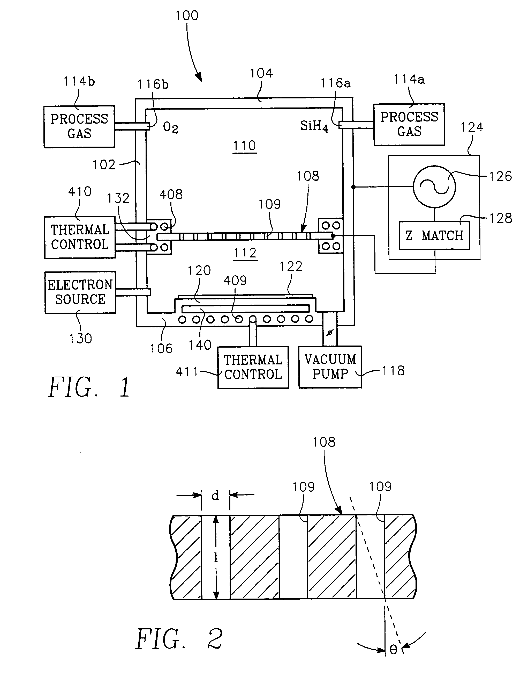
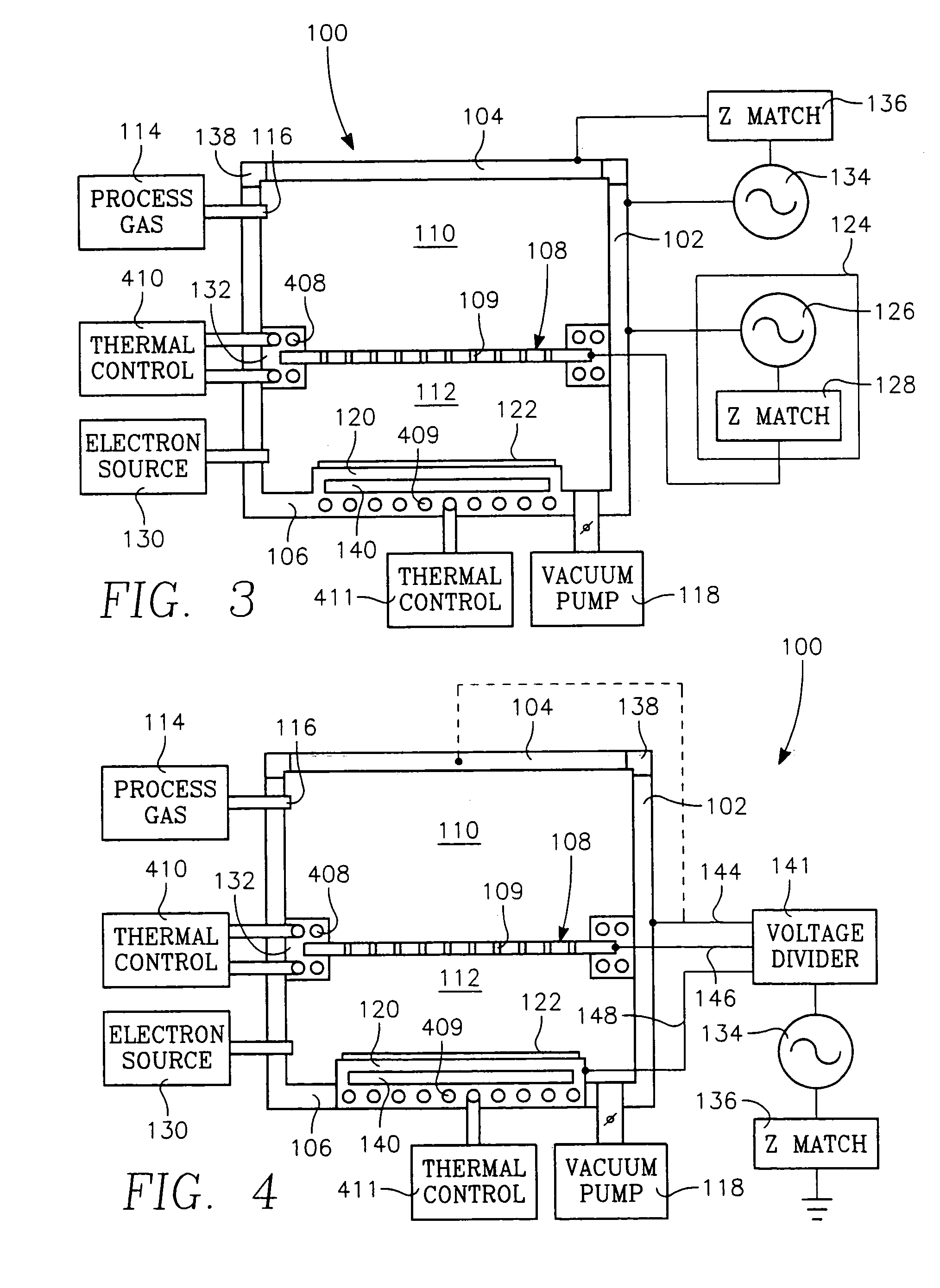
[0050]In a fourth embodiment, the grid voltage source is decoupled from plasma generation by providing a separate plasma source power applicator directed to the upper plasma generation sub-chamber, and may be a reentrant torroidal plasma source. The plasma potential as well as the plasma source power applicator floats at the potential established by the grid voltage source, which may be in the range of 100 to 5000 volts, and the plasma source power voltage is superimposed (floats) on top of the grid potential. By thus decoupling plasma source power from the grid voltage, independent control may be exerted over the plasma ion density and the ion acceleration or grid potential. The grid potential determines the ion velocity profile as well as the ion / neutral population ratio in the lower sub-chamber. For example, at the highest grid voltage, ions are energetically pulled from the plasma in the upper sub-chamber to the lower sub-chamber with a minimum proportion of neutrals. At a minim...


PUM

PropertyMeasurementUnit
temperatureaaaaaaaaaa
feature sizesaaaaaaaaaa
temperatureaaaaaaaaaa

Abstract

A plasma reactor for processing a semiconductor workpiece includes a reactor chamber and a set of plural parallel ion shower grids that divide the chamber into an upper ion generation region and a lower reactor region, each of the ion shower grids having plural orifices in mutual registration from grid to grid, each orifice being oriented in a non-parallel direction relative to a surface plane of the respective ion shower grid. A workpiece support in the process region faces the lowermost one of the ion shower grids. A reactive species source furnishes into the ion generation region a chemical vapor deposition precursor species. The reactor further includes a vacuum pump coupled to the reactor region, a plasma source power applicator for generating a plasma in the ion generation region and a grid potential source coupled to the set of ion shower grids. The orifices through at least some of the ion shower grids have an aspect ratio sufficient to limit ion trajectories in the reactor region to a narrow angular range about the non-parallel direction, and a resistance to gas flow sufficient to support a pressure drop between the ion generation and reactor regions of about at least a factor of 4. The grid potential source can be capable of applying different voltages to different ones of the grids.

Description

CROSS-REFERENCE TO RELATED APPLICATIONS[0001]This application claims priority of U.S. Provisional Application Ser. No. 60 / 556,935, filed Mar. 26, 2004 entitled PLASMA REACTOR AND PROCESS USING ION SHOWER by Hiroji Hanawa, et al. and assigned to the present assignee.[0002]This application contains subject matter related to U.S. application Ser. No. 10 / 873,485 filed Jun. 22, 2004 entitled CHEMICAL VAPOR DEPOSITION PLASMA PROCESS USING AN ION SHOWER GRID by Hiroji Hanawa, et al.; U.S. application Ser. No. 10 / 873,600 filed Jun. 22, 2004 entitled CHEMICAL VAPOR DEPOSITION PLASMA PROCESS USING PLURAL ION SHOWER GRIDS by Hiroji Hanawa, et al.; U.S. application Ser. No. 10 / 873,602 filed Jun. 22, 2004 entitled REACTIVE SPUTTER DEPOSITION PLASMA PROCESS USING AN ION SHOWER GRID by Hiroji Hanawa et al.; U.S. patent application Ser. No. 10 / 873,609 filed Jun. 22, 2004 entitled REACTIVE SPUTTER DEPOSITION PLASMA REACTOR AND PROCESS USING PLURAL ION SHOWER GRIDS by Hiroji Hanawa et al.; U.S. paten...

Claims


Application Information

Patent Timeline
Patent Type & Authority Patents(United States)
IPC IPC(8): C23F1/00C23C16/48C23C16/505H01L21/306C23C16/06C23F1/12H01L21/3065C23C14/35C23C16/00C23C16/04C23C16/507H01J37/32
CPCC23C14/358C23C16/045H01J37/32449H01J37/32357C23C16/507
Inventor HANAWA, HIROJITANAKA, TSUTOMUCOLLINS, KENNETH S.AL-BAYATI, AMIRRAMASWAMY, KARTIKNGUYEN, ANDREW
Owner APPLIED MATERIALS INC
Why Eureka
Try Eureka