Semiconductor memory device which includes memory cell having charge accumulation layer and control gate
a memory cell and memory technology, applied in the field of semiconductor memory devices, can solve problems such as difficulty in controlling the charge pump circui
- Summary
- Abstract
- Description
- Claims
- Application Information
AI Technical Summary
Benefits of technology
Problems solved by technology
Method used
Image


Examples
1st embodiment
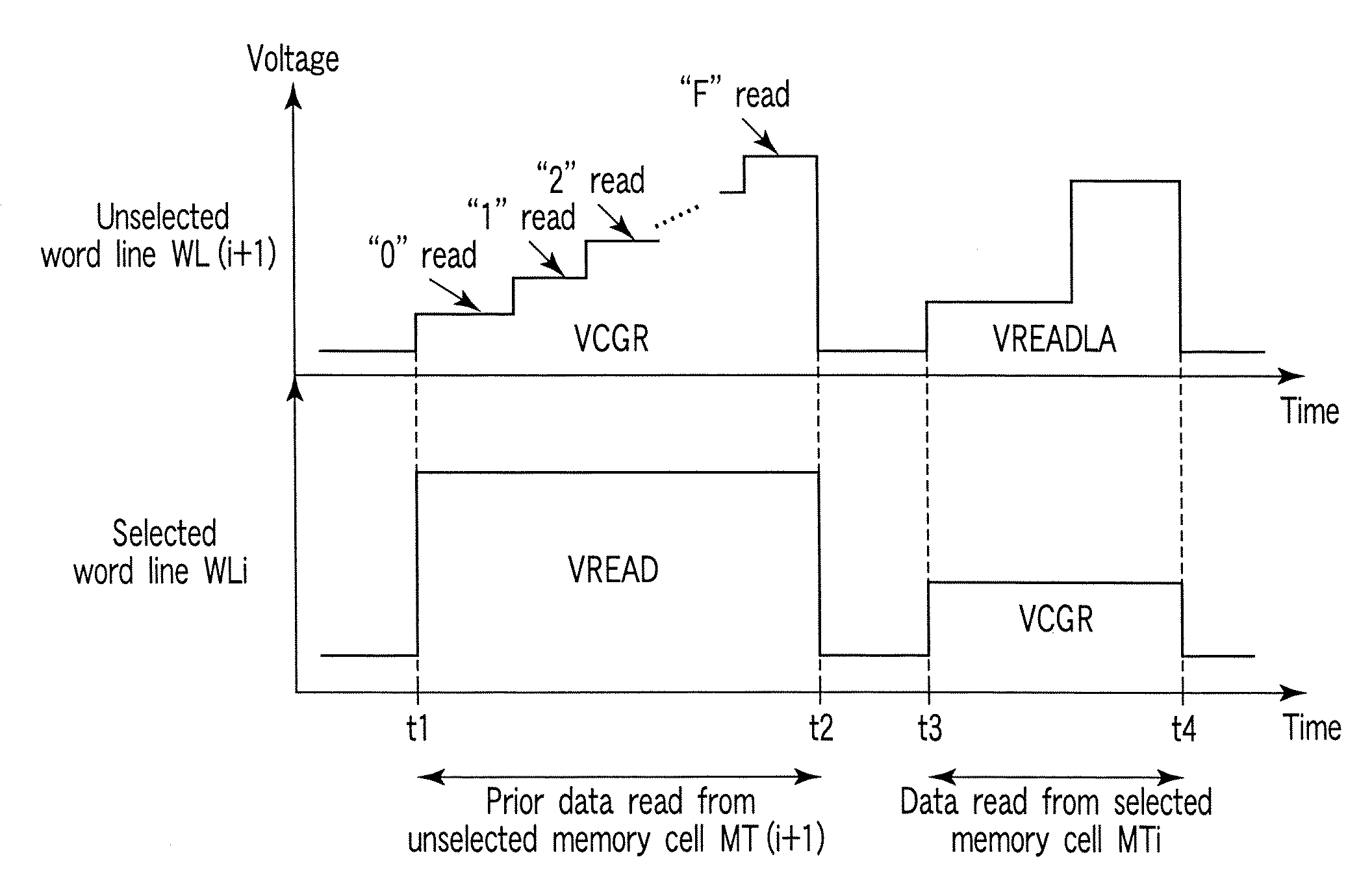
[0034]Description will be given of a semiconductor memory device in accordance with a first embodiment of the present invention. FIG. 1 is a block diagram of the NAND flash memory in accordance with the present embodiment.
[0035]As shown in the figure, the NAND flash memory 1 includes a memory cell array 10, a sense amplifier 20, a source line driver 30, a row decoder 40, a driver circuit 50, a voltage generator 60, and a control circuit 70.
[0036]First, the memory cell array 10 will be described. The memory cell array 10 includes a plurality of memory cell units 11. Each of the memory cell units 11 includes, for example, 32 memory cell transistors MT and select transistors ST1 and ST2. Each of the memory cell transistors MT includes a stack gate structure having a charge accumulation layer (for example, a floating gate) formed on a semiconductor substrate with a gate insulating film interposed therebetween and a control gate electrode formed on the charge accumulation layer with an i...
2nd embodiment
[0115]Now, description will be given of a semiconductor memory device in accordance with a second embodiment of the present invention. In the present embodiment, in addition to voltage VPASS, voltage VPASSL is used as the voltage to be applied to the unselected word lines during the write operation. The configuration and basic operation of the NAND flash memory in accordance with the present embodiment are the same as those in the first embodiment and will thus not be described below. Only differences from the first embodiment will be described below. FIGS. 13 to 15 are block diagrams of the voltage generator 60 during the write operation. Voltage VPASSL satisfies the relationship 0<VPASSL<VPASS. Of course, like voltage VPASS, voltage VPASSL allows the memory cell transistor MT to be turned on.
[0116]FIG. 13 shows that voltage VPASSL is applied to 1 to 10 of the 31 unselected word lines WL, with voltage VPASS applied to the remaining unselected word lines WL (that is, 20 to 29 unsele...
3rd embodiment
[0125]Now, description will be given of a semiconductor memory device in accordance with a third embodiment of the present invention. The present embodiment relates to the details of the voltage generator in the first embodiment or the second embodiment. The basic configuration and operation of the NAND flash memory in accordance with the present embodiment are the same as those in the first embodiment and will thus not be described below. Only differences from the first and second embodiments will be described below. FIG. 16 is a circuit diagram of the voltage generator 60 provided in the NAND flash memory in accordance with the present embodiment, particularly showing system generating voltages VPASSH and VREADLA.
[0126]As shown in FIG. 16, the voltage generator 60 includes not only the first charge circuit 61, described above, but also a pump control circuit 64, a limiter circuit 65, a comparator 66, and n-channel MOS transistors 67 and 68.
[0127]The first charge pump circuit 62 de...
PUM
 Abstract
Description
Claims
Application Information