Infrared sensor unit and process of fabricating the same

a technology of infrared sensor and manufacturing process, which is applied in the direction of optical radiation measurement, radiation control device, instruments, etc., can solve the problems of inability to compact infrared sensor unit, inability to assemble sensor unit densely, and inability to immediately upwardly dispense infrared sensor of semiconductor device upwards

Inactive Publication Date: 2010-05-04
MATSUSHITA ELECTRIC WORKS LTD
View PDF10 Cites 13 Cited by
  • Summary
  • Abstract
  • Description
  • Claims
  • Application Information

AI Technical Summary

Benefits of technology

[0003]In view of the above problem, the present invention has been achieved to provide an improved infrared sensor unit which is capable of being made compact in combination with an associated semiconductor device formed in a common semiconductor substrate. The infrared sensor unit in accordance with the present invention includes the semiconductor substrate configured to be formed in its top surface with a semiconductor device and to be covered on its top surface with a dielectric top layer concealing the semiconductor device, and a sensor mount carrying a thermal infrared sensor. A thermal insulation support is included to support the sensor mount above the semiconductor device. Both of the sensor mount and the thermal insulation support is made of a porous material which is superimposed on top of the dielectric top layer. Thus, the infrared sensor can be successfully disposed above the semiconductor device with sufficient thermal insulation therefrom, thereby making the whole infrared sensor unit compact sufficient to enable an application where a plurality of infrared sensor unit are arranged closely in a two-dimensional array.
[0004]Preferably, the thermal insulation support comprises a pair of posts projecting on the dielectric top layer and a pair of horizontal beam each extending from each of the posts and joining to the sensor mount in a parallel relation with a top plane of the dielectric top layer so as to support the sensor mount in a spaced relation from the semiconductor device. By provision of the posts, the infrared sensor carried on the sensor mount is spaced upwardly by a sufficient distance from the semiconductor device for assuring sufficient thermal isolation of the infrared sensor from the semiconductor substrate and the semiconductor device.
[0005]The dielectric top layer may be formed with an infrared reflector which reflects an infrared ray passing through the infrared sensor back to the infrared sensor in order to enhance sensitivity of the infrared sensor.
[0006]Also, an infrared ray absorber may be is provided to cover the top surface of the infrared sensor alone or in combination with the infrared reflector in order to enhance the sensitivity of the infrared sensor.

Problems solved by technology

However, there remains a problem that the infrared sensor cannot be disposed immediately upwardly of the semiconductor device since the thermal insulation support is only made by anodizing the top surface of the semiconductor substrate at a portion horizontally spaced away from the semiconductor device.
Due to this limitation, the infrared sensor unit is difficult to be made compact.
Especially, when a plurality of the infrared sensor units are arranged in a two-dimensional array to constitute a thermal image sensor, the sensor units cannot be densely packed and therefore suffer from lowered resolution.

Method used


Image

  • Infrared sensor unit and process of fabricating the same
  • Infrared sensor unit and process of fabricating the same
  • Infrared sensor unit and process of fabricating the same

Examples


Embodiment Construction

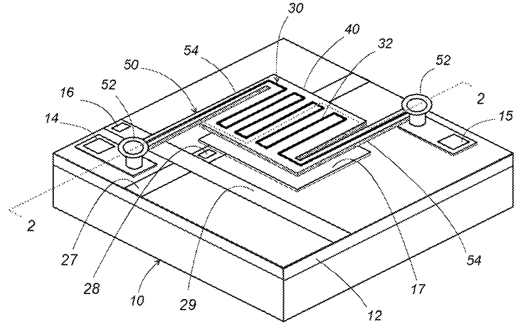
[0017]Referring now to FIGS. 1 and 2, there is shown an infrared sensor unit in accordance with a first embodiment of the present invention. The infrared sensor unit includes a semiconductor device 20 formed in the top surface of a semiconductor substrate 10 of monocrystal silicon and a thermal infrared sensor 30 supported to the substrate 10 in a spaced relation with the semiconductor device 20. The semiconductor device 20 is electrically coupled to the infrared sensor 30 to provide a sensor output to an external processing circuit where the sensor output is analyzed in terms of the amount the infrared radiation received at the infrared sensor 30 for temperature measurement or determination of presence of an object emitting the infrared radiation. One typical application is to arrange a plurality of the infrared sensor unit in a two-dimensional array to constitute a thermal image sensor.

[0018]The semiconductor device 20 is, for instance, a MOSFET transistor which is turned on and o...


PUM


Abstract

An infrared sensor unit has a thermal infrared sensor and an associated semiconductor device commonly developed on a semiconductor substrate. A dielectric top layer covers the substrate to conceal the semiconductor device formed in the top surface of the substrate. The thermal infrared sensor carried on a sensor mount which is supported above the semiconductor device by means of a thermal insulation support. The sensor mount and the support are made of a porous material which is superimposed on top of the dielectric top layer.

Description

TECHNICAL FIELD[0001]The present invention is directed to an infrared sensor unit, more particularly to such unit including a thermal infrared sensor and an associated semiconductor device formed on a common semiconductor substrate, and a process of fabricating the infrared sensor unit.BACKGROUND ART[0002]U.S. Pat. No. 6,359,276 discloses an infrared sensor unit composed of a thermal infrared sensor and a semiconductor device which are arranged in a side-by-side relation on top of a semiconductor substrate. The thermal infrared sensor is supported in the semiconductor substrate by means of porous thermal insulation support. The porous thermal insulation support is realized as a part of the semiconductor substrate for mounting thereon the infrared sensor in a thermally insulating relation from the remainder of the substrate. The porous thermal insulation support is composed of a sensor mount and a set of porous bridges connecting the sensor mount to the substrate. Each of the sensor ...

Claims


Application Information

Patent Timeline
Patent Type & Authority Patents(United States)
IPC IPC(8): G01J5/20
CPCG01J5/10H01L31/103G01J5/20H01L31/0284H01L27/146
Inventor YAMANAKA, HIROSHIICHIHARA, TSUTOMUWATABE, YOSHIFUMITSUJI, KOJIKIRIHARA, MASAOYOSHIHARA, TAKAAKINISHIJIMA, YOICHIHYODO, SATOSHI
Owner MATSUSHITA ELECTRIC WORKS LTD
Why Eureka
Try Eureka