Large substrate structural vias

a technology of large substrates and vias, applied in the direction of semiconductor devices, semiconductor/solid-state device details, electrical devices, etc., can solve the problems of large changes in the temperature of devices, fatigue of the package and the structure including the package, and the device can change the temperature depending, so as to reduce thermal fatigue failure

Active Publication Date: 2010-05-04
MICROSS ADVANCED INTERCONNECT TECH LLC
View PDF14 Cites 2 Cited by
  • Summary
  • Abstract
  • Description
  • Claims
  • Application Information

AI Technical Summary

Benefits of technology

[0014]According to another embodiment of the present invention, a method for reducing thermal fatigue failure due to heat cycling in an electronic package includes thermal cycling a conducting layer on a carrier substrate having a length and a width extending laterally in two dimensions across a major part of the first surface of the carrier substrate, and securing the conducting layer to the carrier substrate by plural via conductors disposed in plural of the vias, the via conductors connecting the conducting layer to the carrier substrate.

Problems solved by technology

The large amount of power results in large changes in the temperature of the devices.
In addition, these devices can change temperature depending on the level of activity, low and high level of computation in a processor.
These extensive and repeated temperature changes cause fatigue of the package and the structure including the package.
An electronic package may then fail due to this fatigue.
When one considers building a large area silicon substrate to act as a PCB, it is known by those skilled in the art that the conductors will delaminate or crack due to repeated thermal cycles.
However, the new computing devices, by packaging many active elements on a same substrate or multiple substrates stacked together and due to intense computational activity, are producing a large amount of heat that impacts negatively the bonds between the carrier substrate and the conducting layers, which form the power planes and / or the electrical wires.
As a result of this repeated thermal stress, the power planes / electrical wires tend to delaminate from the substrate, resulting in a failed structure, as discussed above.

Method used


Image

  • Large substrate structural vias
  • Large substrate structural vias
  • Large substrate structural vias

Examples


Embodiment Construction

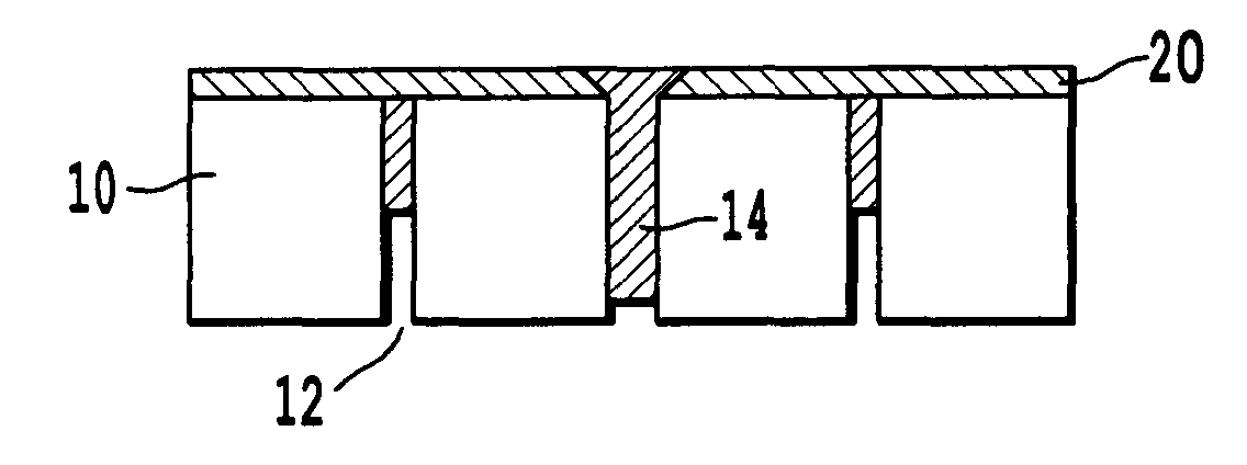
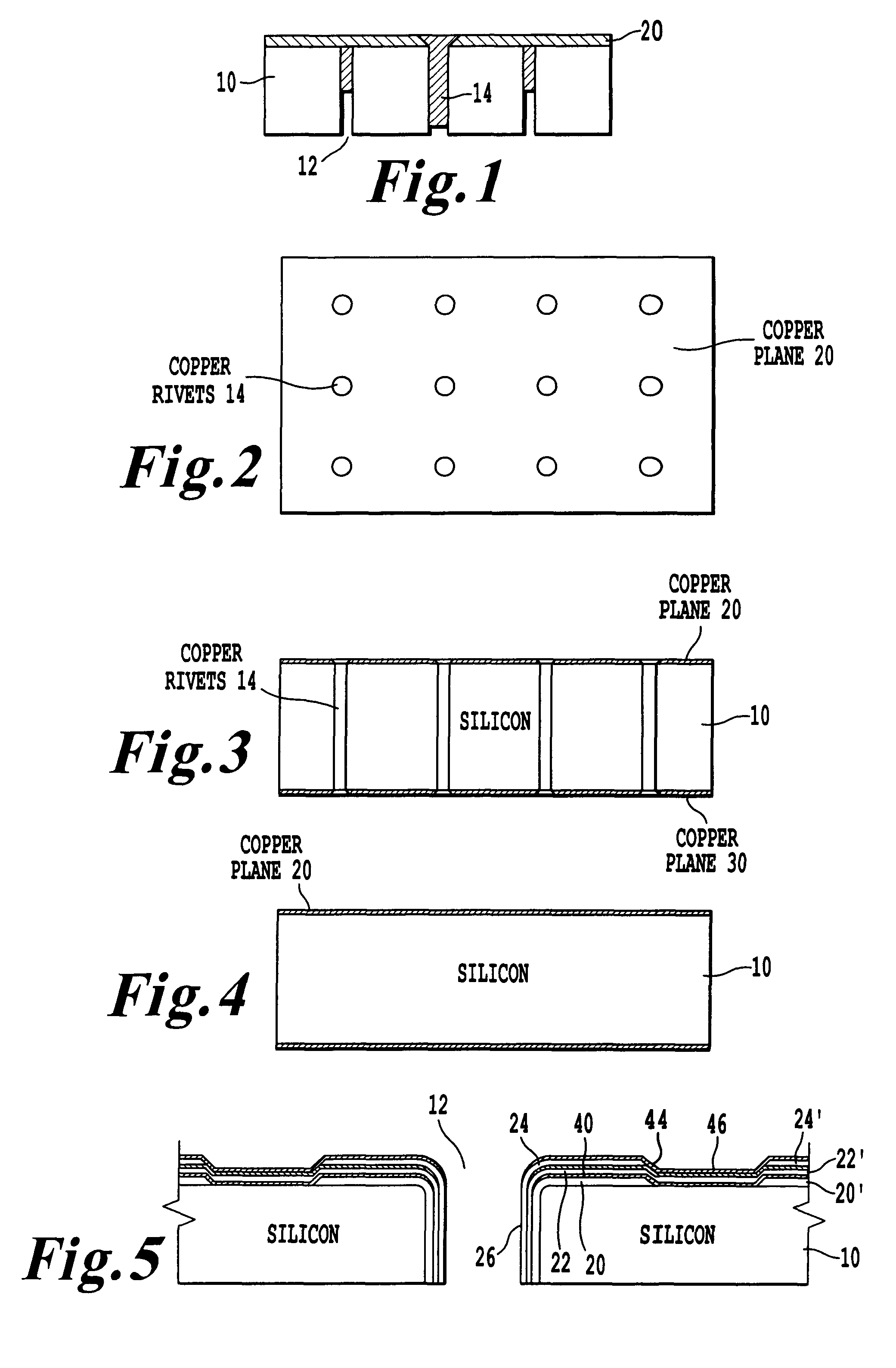
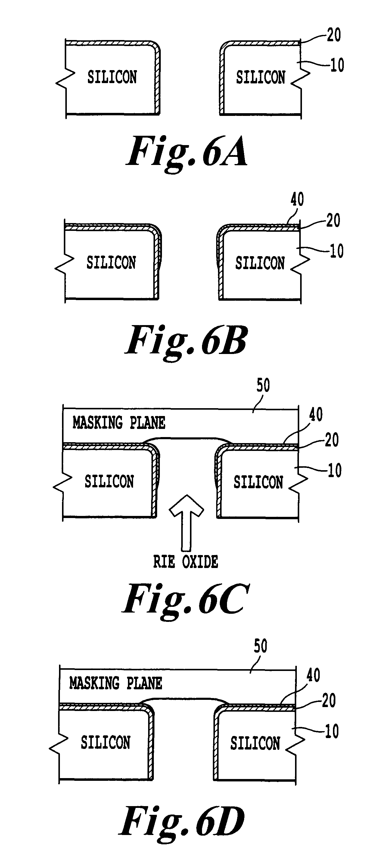
[0026]Referring now to the drawings, wherein like reference numerals designate identical or corresponding parts throughout the several views, and more particularly to FIG. 1 thereof, FIG. 1 shows a side view through a carrier substrate 10 having at least a conducting layer 20 formed on a first main surface of the carrier substrate 10. Passive components (as capacitors, resistors, and inductors) may be formed within the carrier substrate.

[0027]According to an embodiment, the carrier substrate 10 is a silicon substrate and the conducting layer 20 is a copper layer. The conducting layer 20 may also be any known conductor material. The conducting layer 20 has good thermal and / or electrical properties. For example, in one embodiment, the substrate 10 is made of silicon that has a thermal conductivity of 149 W / m / K and a coefficient of thermal expansion of 2.6 μ / m / K and the conducting layer 20 is made of copper that has a thermal conductivity of 401 W / m / K and a coefficient of thermal expan...


PUM

PropertyMeasurementUnit
diameteraaaaaaaaaa
diameteraaaaaaaaaa
thermal conductivityaaaaaaaaaa

Abstract

An electronic package and methods by which the package reduces thermal fatigue failure of conductors in the electronic package. The electronic package includes a carrier substrate having first and second surfaces and a plurality of anchor vias having a via material extending from the first surface toward the second surface. The electronic package includes a first conducting layer having a length and a width extending laterally in two dimensions across a major part of the first surface of the carrier substrate. The anchor vias have plural attachments along the length and the width of the first conducting layer to secure the first conducting layer to the carrier substrate.

Description

CROSS REFERENCE TO RELATED APPLICATION[0001]This application is related to the following applications: 1) U.S. Non-Provisional Application entitled “Preventing Breakage of Long Metal Signal Conductors on Semiconductor Substrates,” U.S. Ser. No. 11 / 975,058 filed Oct. 16, 2007; 2) U.S. Non-Provisional Application entitled “Local Defect Memories on Semiconductor Substrates in a Stack Computer,” U.S. Ser. No. 11 / 981,853 filed Oct. 31, 2007; 3) U.S. Non-Provisional Application entitled “Comb-Shaped Power Bus Bar Assembly Structure Having Integrated Capacitors,” U.S. Ser. No. 11 / 975,011 filed Oct. 16, 2007; 4) U.S. Provisional Application entitled “Semiconductor Substrate Stack High Performance Computer,” U.S. Ser. No. 60 / 995,195 filed Sep. 25, 2007; and 5) U.S. Non-Provisional Application entitled “Semiconductor Substrate Elastomeric Stack,” U.S. Ser. No. 11 / 975,007 filed Oct. 16, 2007. The contents of all these applications are incorporated by their entirety herein by reference.BACKGROU...

Claims


Application Information

Patent Timeline
Patent Type & Authority Patents(United States)
IPC IPC(8): H01L23/48
CPCH01L21/486H01L23/147H01L23/49827Y10T29/49165H01L2924/14H01L2924/1433H01L2924/15165H01L2924/157H01L2924/19041H01L2924/19042H01L2924/19043H01L2924/0002Y10T29/49117H01L2924/00
Inventor CONN, ROBERT O.
Owner MICROSS ADVANCED INTERCONNECT TECH LLC
Why Eureka
Try Eureka