Semiconductor chip package and method for manufacturing the same

a semiconductor and chip technology, applied in the direction of semiconductor devices, semiconductor/solid-state device details, electrical apparatus, etc., can solve the problems of bga packages that utilize solder balls to electrically couple the packaged integrated circuit to the main pcb, the integrated circuit packaging technology is becoming a limiting factor for the development of packaged integrated circuits of higher performance, and the pin count increase is difficult to keep up with the increase in pin coun

Active Publication Date: 2007-04-19
ADVANCED SEMICON ENG INC
View PDF15 Cites 2 Cited by
  • Summary
  • Abstract
  • Description
  • Claims
  • Application Information

AI Technical Summary

Benefits of technology

[0007] It is an object of the present invention to provide a high-pin-count BGA package which allows the stresses on the solder balls located in the periphery of the package resulted from CTF mismatch to be significantly decreased thereby ensuring the solder joint reliability thereof.
[0008] It is another object of the present invention to provide a semiconductor chip package with high heat-dissipation efficiency such that the heat generated from the semiconductor chip can be dissipated into the external environment thereby reducing the fatigue failure of the package.
[0009] A semiconductor chip package in accordance with the present invention mainly includes an interconnection substrate, a peripheral substrate with an opening, a central substrate disposed in the opening of the peripheral substrate, a semiconductor chip sandwiched between the interconnection substrate and the central substrate, and a plurality of solder balls respectively disposed on the bottom surfaces of the central substrate and the peripheral substrate. The interconnection substrate has a recessed cavity for receiving the semiconductor chip. The present invention is characterized in that the peripheral substrate is substantially separated from the central substrate thereby decreasing the stresses on the package due to CTE mismatch of the semiconductor chip package.
[0016] The semiconductor chip package of the present invention utilizes a cavity-down structure which includes a semiconductor chip with its backside surface directly bonded to an interconnection substrate with high heat-dissipation efficiency. Therefore, the heat generated during the operation of the chip can be quickly dissipated out of the package thereby reducing the stresses on the package due to the temperature fluctuation.
[0017] The present invention further provides a semiconductor chip package and a substrate for use therein. The package includes a substrate, a chip disposed on a top surface of a substrate and a plurality of central solder balls and peripheral solder balls disposed on the bottom surface of the substrate. The substrate includes a plurality of chip bonding pads disposed on the top surface of the substrate for electrically connecting to the semiconductor chip. Besides, the substrate includes a plurality of central contact pads and peripheral contact pads disposed on the bottom surface of the substrate, and a plurality of slots disposed between the central contact pads and the peripheral contact pads for separating the central contact pads and the peripheral contact pads. The central contact pads are electrically connected to the chip bonding pads. The peripheral contact pads are preferably connected to the chip bonding pads. The central solder balls of the package are disposed on the central contact pads, and the peripheral solder balls are disposed on the peripheral contact pads. Although the aformentioned substrate is not completely divided into two separate substrates, the slots on the substrate can act as a buffer area between the central solder balls and the peripheral solder balls thereby helping to reduce the stresses due to the temperature fluctuation.

Problems solved by technology

Integrated circuit (chip) packaging technology is becoming a limiting factor for the development in packaged integrated circuits of higher performance.
Semiconductor package designers are struggling to keep pace with the increase in pin count, size limitations, low profile mounting constraints, and other evolving requirements for packaging and mounting integrated circuits.
Any BGA package that utilizes solder balls to electrically couple the packaged integrated circuit to a main PCB is susceptible to failure, particularly fatigue failure, due to temperature fluctuations and dissimilarity in thermal expansion rates for the components that form the BGA package.
Specifically, as the BGA package cools down from the solder reflow temperature or undergoes ambient temperature changes during use, the BGA package experiences thermal deformation of different rates in different portions, thereby stressing and straining solder balls.
Especially, as the pin count grows, the distance between the center and the farthest solder ball of the package, the “distance to the neutral point” (DNP), grows longer and thus the stresses on these outer solder balls cause cracking during thermal cycling.
Furthermore, electrical current flowing through the BGA package during operation causes the BGA package to cyclically or intermittently heat up and cool down, which results in additional thermal expansion and contraction, nevertheless such thermal expansion and contraction is considerably less than those at reflow.
The stresses from the cyclical or intermittent heating and cooling of the BGA package during normal operation may lead to fatigue failure of the BGA package if the stresses are not properly released.

Method used


Image

  • Semiconductor chip package and method for manufacturing the same
  • Semiconductor chip package and method for manufacturing the same
  • Semiconductor chip package and method for manufacturing the same

Examples


Embodiment Construction

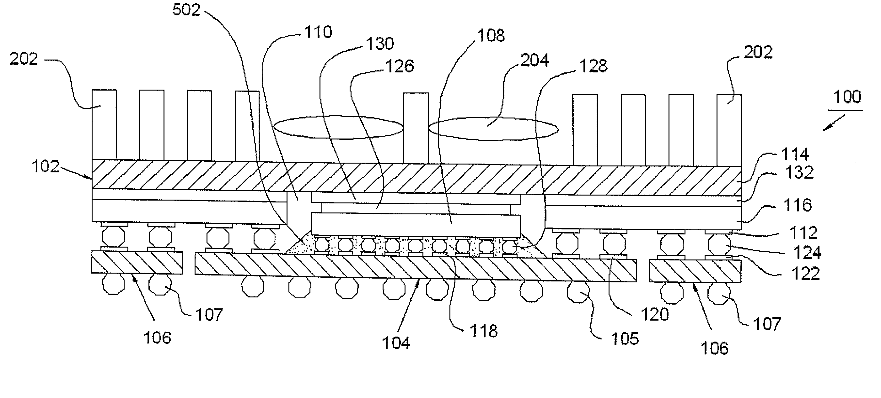
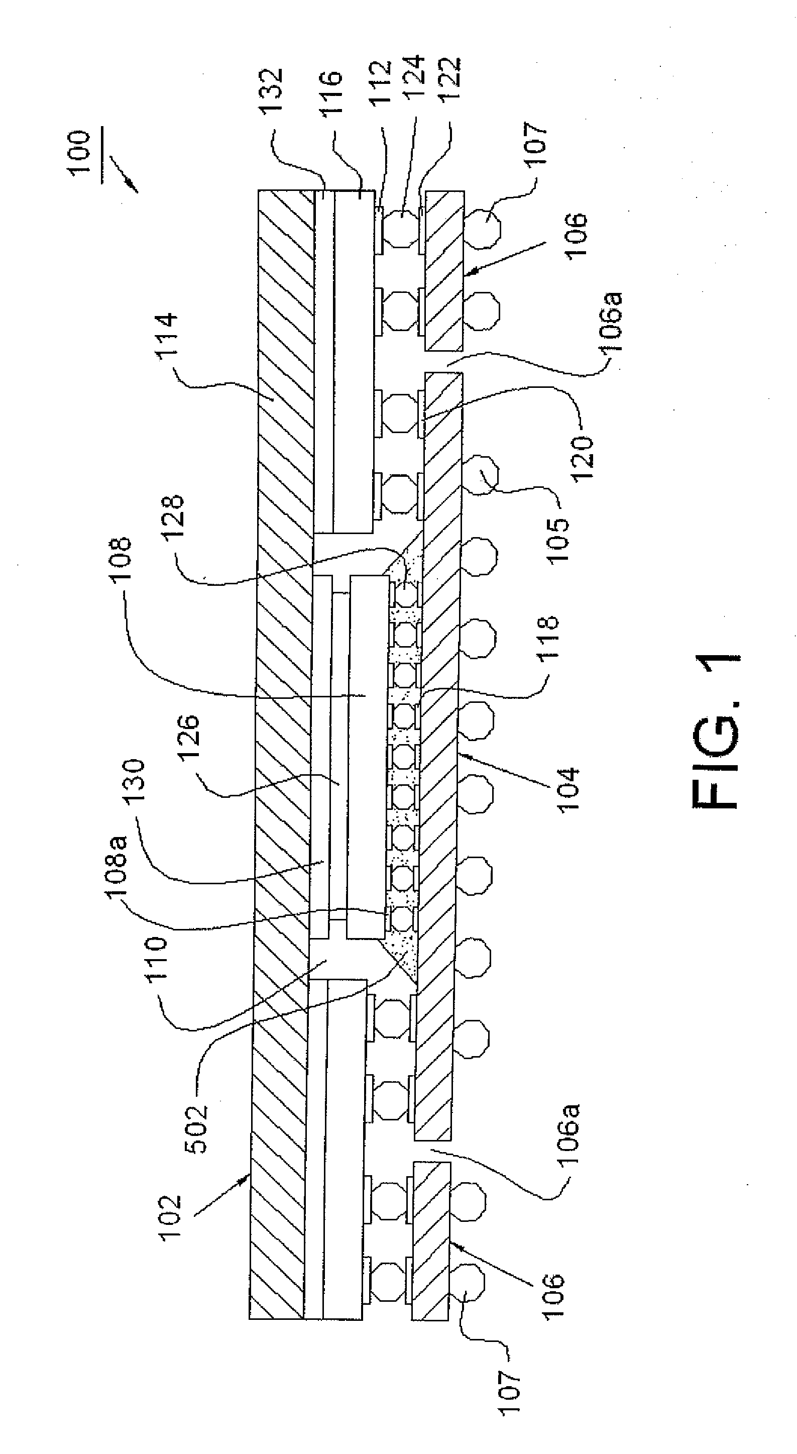
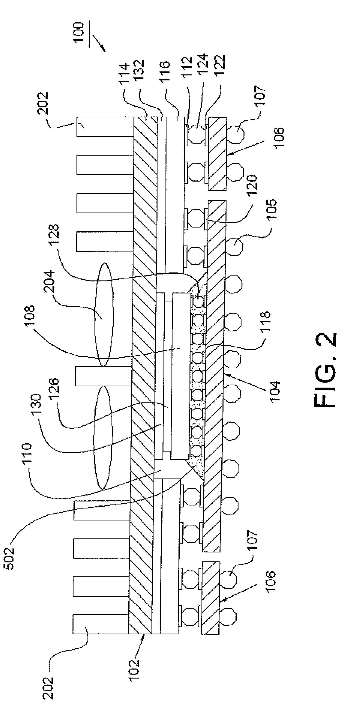
[0027]FIG. 1 illustrates a semiconductor chip package 100 according to one embodiment of the present invention. The semiconductor chip package 100 generally includes an interconnection substrate 102, a central substrate 104, a peripheral substrate 106, a semiconductor chip 108, a plurality of central solder balls 105 disposed on the bottom surface of the central substrate 104 and a plurality of peripheral solder balls 107 disposed on the bottom surface of the peripheral substrate 106. The peripheral substrate 106 has an opening 106a, and the central substrate 104 is disposed in the opening 106a of the peripheral substrate and substantially coplanar with the peripheral substrate 106.

[0028] The bottom surface of the interconnection substrate 102 has a recessed cavity 110 defined therein and a plurality of contact pads 112 formed around the recessed cavity 110. The interconnection substrate 102 may include a top plate 114, preferably a heat-sink, and a dielectric layer 116. The dielec...


PUM


Abstract

A semiconductor chip package mainly comprises an interconnection substrate, a central substrate, a peripheral substrate and a semiconductor chip sandwiched between the interconnection substrate and the central substrate. The interconnection substrate has a recessed cavity for receiving the semiconductor chip. The present invention is characterized in that the peripheral substrate is separated from the central substrate thereby decreasing the stresses caused by CTE mismatch of the semiconductor chip package. Furthermore, both the central substrate and the peripheral substrate are mechanically and electrically connected to the interconnection substrate such that the semiconductor chip is electrically connected to the peripheral substrate through the central substrate and the interconnection substrate. The present invention further provides a method for manufacturing the semiconductor chip package.

Description

BACKGROUND OF THE INVENTION [0001] 1. Field of the Invention [0002] This invention generally relates to a semiconductor chip package and the method for making the same. [0003] 2. Description of the Related Art [0004] Integrated circuit (chip) packaging technology is becoming a limiting factor for the development in packaged integrated circuits of higher performance. Semiconductor package designers are struggling to keep pace with the increase in pin count, size limitations, low profile mounting constraints, and other evolving requirements for packaging and mounting integrated circuits. Currently, the common packaging and package mounting technology is a ball grid array (BGA) package, in which an array of solder pads for solder balls are formed on the integrated circuit package. Conductive leads or traces on the package connect the solder pads to wire bonding pads for electrically connection to the integrated circuit chip within the package. A corresponding array of solder pads is fo...

Claims


Application Information

Patent Timeline
Patent Type & Authority Applications(United States)
IPC IPC(8): H01L21/00H01L23/02H01L23/36H01L23/498
CPCH01L23/36H01L23/49816H01L2224/32225H01L2924/07811H01L2924/15311H01L2924/01079H01L23/49833H01L23/49838H01L2224/16225H01L2224/73204H01L2224/73253H01L2924/00H01L2224/05568H01L2224/05573H01L2924/00014H01L2224/05599
Inventor TAO, SULEE, SHIH CHANG
Owner ADVANCED SEMICON ENG INC
Why Eureka
Try Eureka