Electron emission device, electron emission display device using the same and method of manufacturing the same

a technology of electron emission display and electron emission, which is applied in the manufacture of electrode systems, electric discharge tubes/lamps, and discharge tubes luminescnet screens, etc., can solve the problems of signal distortion, deterioration of possible occurrence of driving signals, so as to reduce parasitic capacitance, inhibit signal distortion, and improve the emission property of the electron emission region

Inactive Publication Date: 2010-05-04
SAMSUNG SDI CO LTD
View PDF7 Cites 13 Cited by
  • Summary
  • Abstract
  • Description
  • Claims
  • Application Information

AI Technical Summary

Benefits of technology

[0014]It is therefore a feature of an embodiment of the present invention to provide an electron emission device that inhibits signal distortion by reducing the parasitic capacitance generated at the crossed regions of cathode and gate electrodes, a method of manufacturing the electron emission device and an electron emission display using the electron emission device.
[0015]It is therefore another feature of an embodiment of the present invention to provide an electron emission device that can improve the emission property of an electron emission region by reducing a distance between the electron emission region and the gate electrode, a method of manufacturing the electron emission device and an electron emission display using the electron emission device.
[0021]The insulating layer may have upper and lower portions, the upper portion having a higher density than the lower portion. Forming the insulating layer may include depositing the insulating material and increasing a deposition temperature used during forming of the upper portion from that during forming of the lower portion.

Problems solved by technology

Thus, when the electron emission display is driven by the driving signals applied to the cathode and gate electrodes, signal distortion, e.g., retardation of the driving signal, may occur due to the parasitic capacitance.
This increased distance reduces the intensity of the electric field formed around the electron emission region, thereby deteriorating the emission property of the electron emission region.
However, when the thickness of the insulating layer is reduced, the parasitic capacitance at the crossed regions further increases.

Method used


Image

  • Electron emission device, electron emission display device using the same and method of manufacturing the same
  • Electron emission device, electron emission display device using the same and method of manufacturing the same
  • Electron emission device, electron emission display device using the same and method of manufacturing the same

Examples


Embodiment Construction

[0034]Korean Patent Application Nos. 10-2005-0027053, filed on Mar. 31, 2005, 10-2005-0078751, filed on Aug. 26, 2005, and 10-2005-0100192, filed on Oct. 24, 2005, in the Korean Intellectual Property Office, all of which are entitled “Electron Emission Device and Method of Manufacturing the Same,” are incorporated by reference herein their entirety.

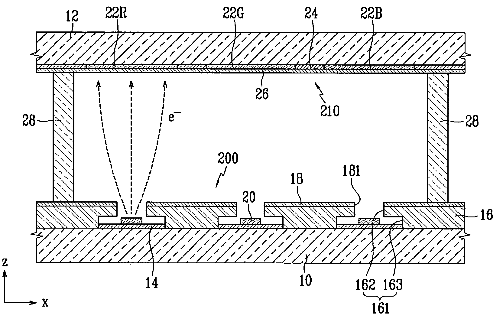
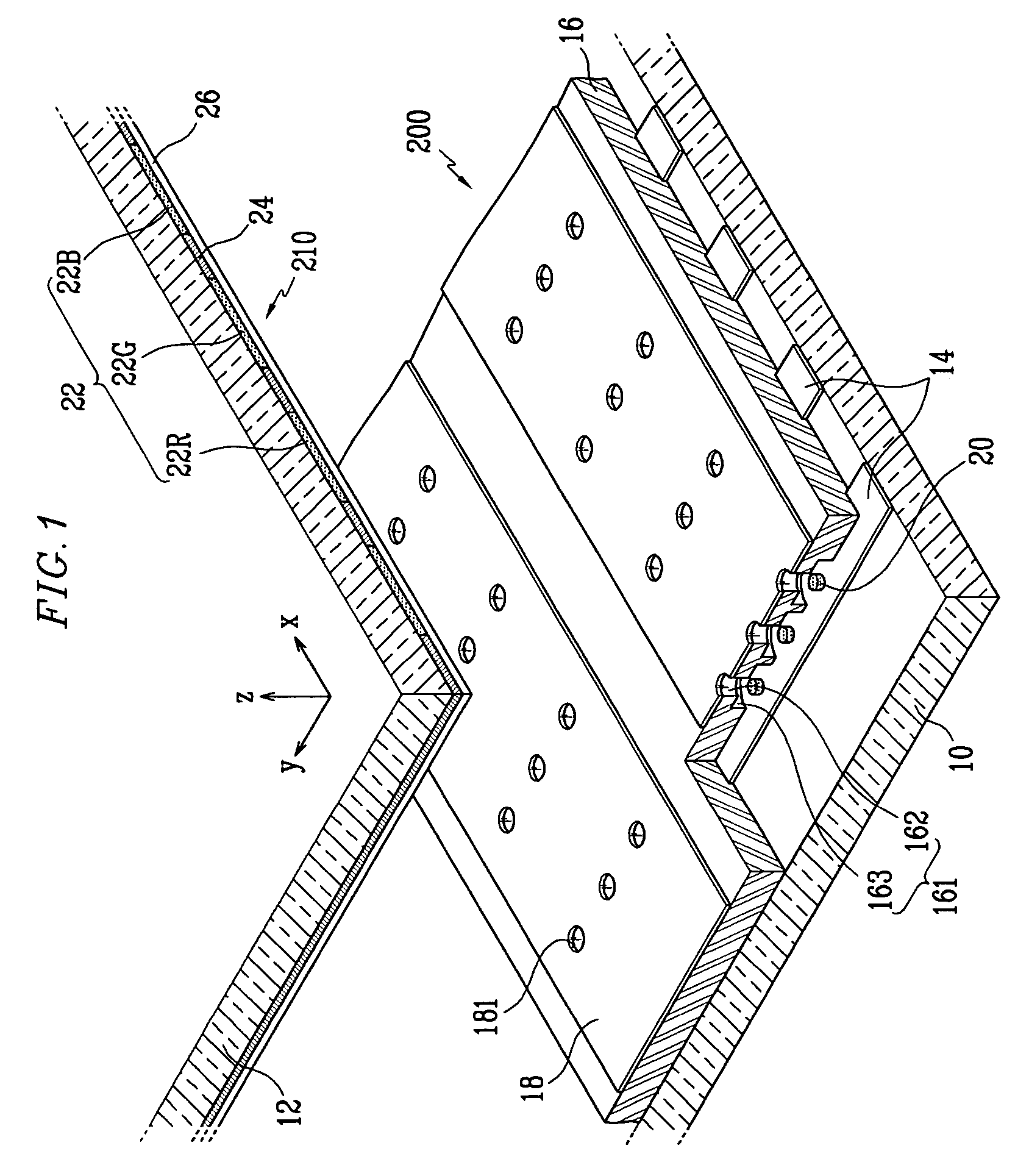
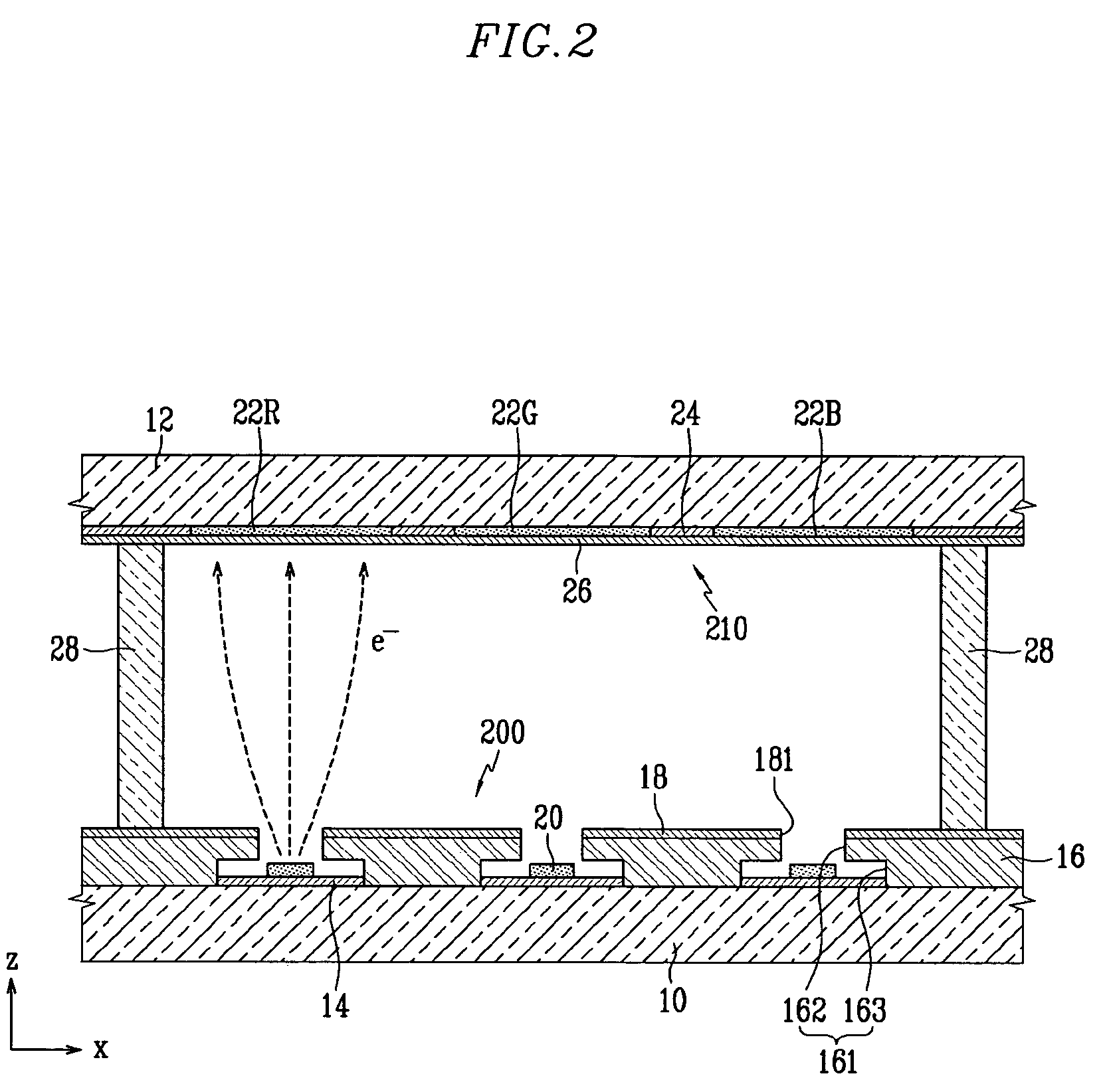
[0035]The present invention will now be described more fully hereinafter with reference to the accompanying drawings, in which exemplary embodiments of the invention are shown. The invention may, however, be embodied in different forms and should not be construed as limited to the embodiments set forth herein. Rather, these embodiments are provided so that this disclosure will be thorough and complete, and will fully convey the scope of the invention to those skilled in the art. In the figures, the dimensions of layers and regions are exaggerated for clarity of illustration. It will also be understood that when a layer is referred to as b...


PUM


Abstract

An electron emission device includes a substrate, a plurality of cathode electrodes formed on the substrate, a plurality of electron emission regions electrically coupled to the cathode electrodes, an insulating layer formed on the substrate while covering the cathode electrodes, and a plurality of gate electrodes formed on the insulating layer and crossing the cathode electrodes. The insulating layer is provided with a plurality of openings exposing the corresponding electron emission regions, each of the openings having at least two opening portions that communicate with each other and are different in a size from each other. The gate electrodes are provided with openings communicating with the corresponding openings of the insulating layer. The two opening portions may include a gap in the insulating layer where the gate and cathode electrodes interesect.

Description

BACKGROUND OF THE INVENTION[0001]1. Field of the Invention[0002]The present invention relates to an electron emission device. More particularly, the present invention relates to an electron emission device that can suppress signal distortion by reducing the parasitic capacitance generated between cathode and gate electrodes while maintaining the emission property of an electron emission region, a method of manufacturing the electron emission device and an electron emission display using the electron emission device.[0003]2. Description of the Related Art[0004]Generally, electron emission elements are classified into those using hot cathodes as an electron emission source and those using cold cathodes as the electron emission source. There are several types of cold cathode electron emission elements, including Field Emitter Array (FEA) elements, Surface-Conduction Emitter (SCE) elements, Metal-Insulator-Metal (MIM) elements and Metal-Insulator-Semiconductor (MIS) elements.[0005]The e...

Claims


Application Information

Patent Timeline
Patent Type & Authority Patents(United States)
IPC IPC(8): H01J1/62
CPCH01J3/021H01J31/127H01J29/481H01J9/025
Inventor LEE, SANG-JOLEE, CHUN-GYOOJEON, SANG-HOAHN, SANG-HYUCKHONG, SU-BONGRYU, KYUNG-SUNSHIN, JONG-HOON
Owner SAMSUNG SDI CO LTD
Why Eureka
Try Eureka